CY28401
CY28401 is 100MHz Differential Buffer manufactured by Silicon Labs.
100 MHz Differential Buffer for PCI Express and SATA
Features
Functional Description
- CK409 or CK410 panion buffer
- Eight differential 0.7V clock pairs
- Individual OE controls
- Low CTC jitter (< 50 ps)
- Programmable bandwidth
- SRC_STOP# power management control
- SMBus Block/Byte/Word Read and Write support
- 3.3V operation
- PLL Bypass-configurable
- Divide by 2 programmable
- 48-pin SSOP package
The CY28401 is a differential buffer and serves as a panion device to the CK409 or CK410 clock generator. The device is capable of distributing the Serial Reference Clock (SRC) in PCI Express and SATA implementations.
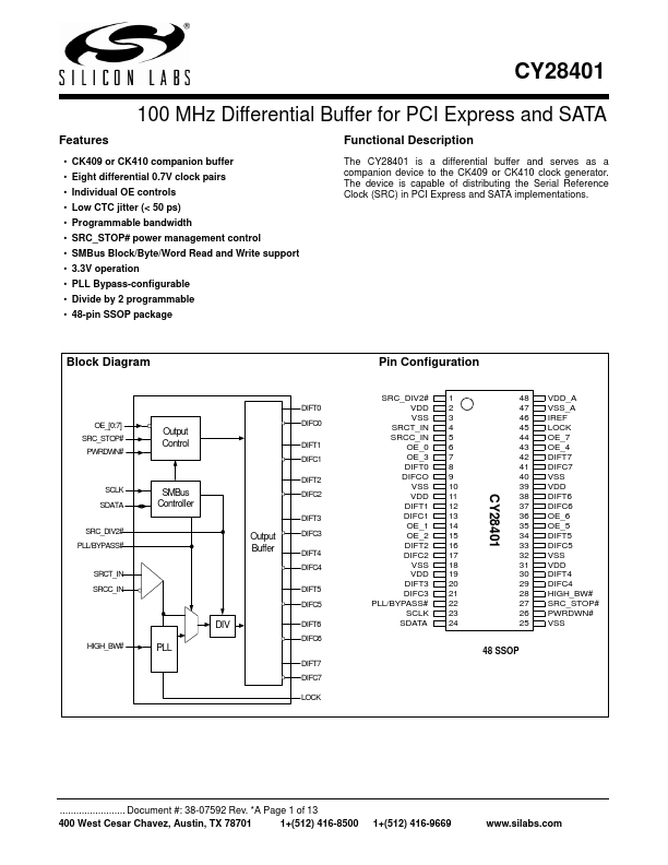
Block Diagram
OE_[0:7] SRC_STOP#
PWRDWN#
SCLK SDATA SRC_DIV2# PLL/BYPASS#
SRCT_IN SRCC_IN
HIGH_BW#
Output Control
SMBus Controller
Output Buffer
DIV PLL
DIFT0 DIFC0
DIFT1 DIFC1
DIFT2 DIFC2
DIFT3 DIFC3
DIFT4...