SI53313
Overview
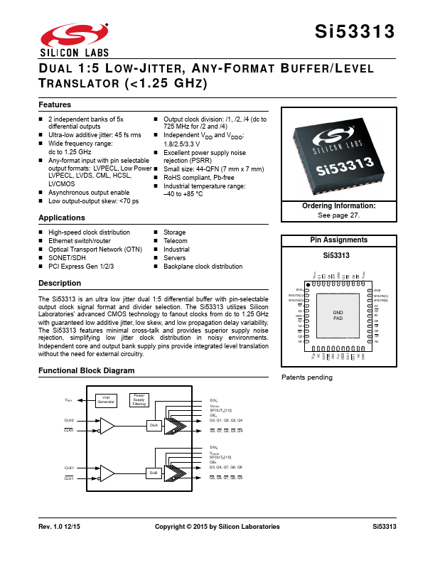
DIVA 1 33 DIVB The Si53313 is an ultra low jitter dual 1:5 differential buffer with pin-selectable SFOUTA[1] 2 SFOUTA[0] 3 32 SFOUTB[1] 31 SFOUTB[0] output clock signal format and divider selection. The Si53313 utilizes Silicon Q2 4 30 Q7 Laboratories' advanced CMOS technology to fanout clocks from dc to 1.25 GHz with guaranteed low additive jitter, low skew, and low propagation delay variability.
- 2 independent banks of 5x
- Output clock division: /1, /2, /4 (dc to differential outputs 725 MHz for /2 and /4)
- Ultra-low additive jitter: 45 fs rms
- Wide frequency range:
- Independent VDD and VDDO: 1.8/2.5/3.3 V dc to 1.25 GHz
- Excellent power supply noise
- Any-format input with pin selectable rejection (PSRR) output formats: LVPECL, Low Power
- Small size: 44-QFN (7 mm x 7 mm)