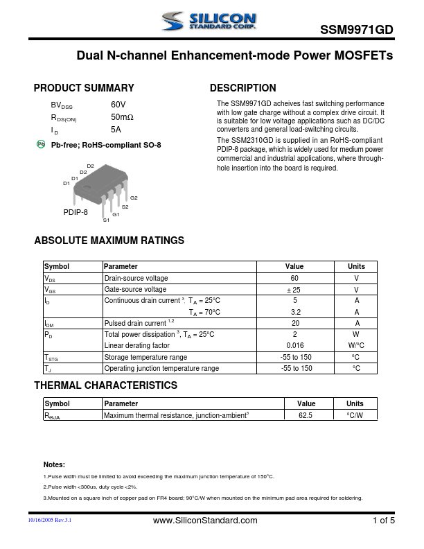
DESCRIPTION
60V 50mΩ 5A Pb-free; RoHS-compliant SO-8 D2 D2 D1 D1 G2 PDIP-8 S1 S2 G1 ABSOLUTE MAXIMUM RATINGS
Symbol VDS VGS ID IDM PD TSTG TJ Parameter Drain-source voltage Gate-source voltage Continuous drain current Pulsed drain current 1,2 3 3 , Value 60 ± 25 T A = 25°C TA = 70°C 5 3.2 20 2 0.016 -55 to 150 -55 to 150 Units V V A A A W W/°C °C °C Total power dissipation , TA = 25°C Linear derating factor Storage temperature range Operating junction temperature range THERMAL CHARACTERISTICS Symbol RΘJA Parameter Maximum thermal resistance, junction-ambient 3 Value 62.5 Units °C/W Notes: 1.Pulse width must be limited to avoid exceeding the maximum junction temperature of 150°C. 2.Pulse width <300us, duty cycle <2%. 3.Mounted on a square inch of copper pad on FR4 board; 90°C/W when mounted on the minimum pad area required for soldering. 10/16/2005 Rev.3.1 1 of 5 SSM9971GD ELECTRICAL CHARACTERISTICS
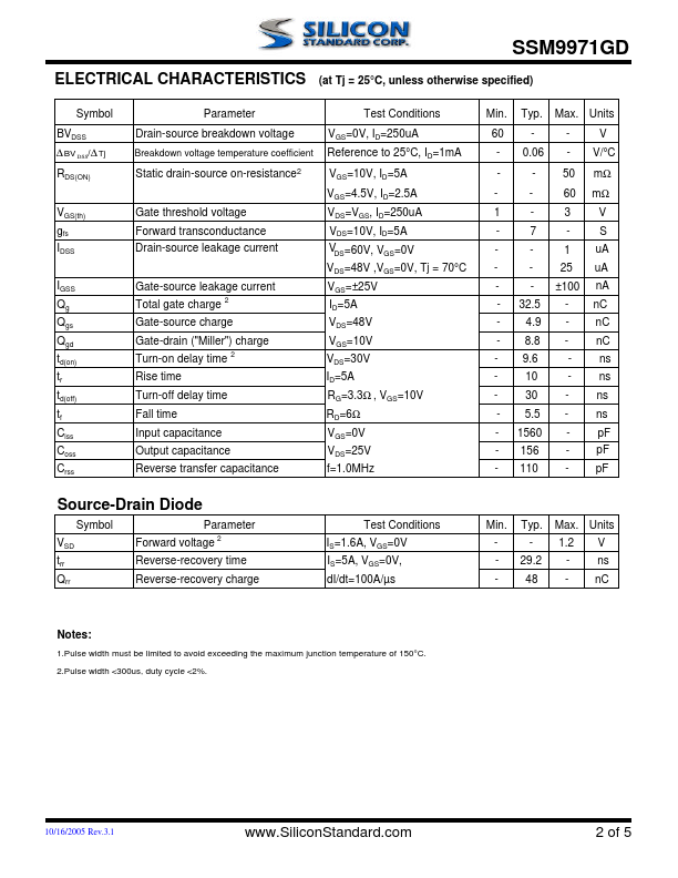
Symbol BVDSS Parameter Drain-source breakdown voltage Breakdown voltage temperature coefficient (at Tj = 25°C, unless otherwise specified) Test Conditions VGS=0V, ID=250uA Reference to 25°C, ID=1mA VGS=10V, ID=5A VGS=4.5V, ID=2.5A Min. Silicon Standard