SSM4226GM
SSM4226GM is DUAL N-CHANNEL ENHANCEMENT-MODE POWER MOSFET manufactured by Silicon Storage Technology.
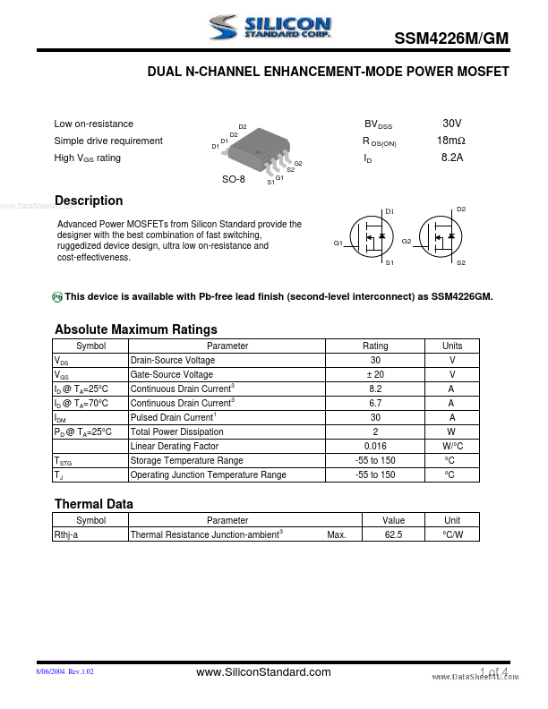
Description
D1
D2
Advanced Power MOSFETs from Silicon Standard provide the designer with the best bination of fast switching, ruggedized device design, ultra low on-resistance and cost-effectiveness.
G1 S1
G2 S2
This device is available with Pb-free lead finish (second-level interconnect) as SSM4226GM.
Absolute Maximum Ratings
Symbol VDS VGS ID @ TA=25°C ID @ TA=70°C IDM PD @ TA=25°C TSTG TJ Parameter Drain-Source Voltage Gate-Source Voltage Continuous Drain Current Continuous Drain Current Pulsed Drain Current
1 3 3
Rating 30 ± 20 8.2 6.7 30 2 0.016 -55 to 150 -55 to 150
Units V V A A A W W/°C °C °C
Total Power Dissipation Linear Derating Factor Storage Temperature Range Operating Junction Temperature Range
Thermal Data
Symbol Rthj-a Parameter Thermal Resistance Junction-ambient
Value Max. 62.5
Unit °C/W
8/06/2004 Rev.1.02
.Silicon Standard.
1 of 4
SSM4226M/GM
Electrical Characteristics @ Tj=25o C (unless otherwise specified)
Symbol BVDSS Parameter Drain-Source Breakdown Voltage Test Conditions VGS=0V, ID=250u A Min. 30 1 Typ. 0.03 15 20 5 12 12 8 31 12 320 230 Max. Units 18 28 3 1 25 ±100 30 V V/°C mΩ mΩ V S u A u A n A n C n C n C ns ns ns ns p F p F p F
∆ B VDSS/∆ Tj
RDS(ON)
Breakdown Voltage Temperature Coefficient Reference to 25°C, ID=1m A
Static Drain-Source On-Resistance 2
VGS=10V, ID=6A VGS=4.5V, ID=4A
VGS(th) gfs
DSS ..
Gate Threshold Voltage Forward Transconductance
Drain-Source Leakage Current (Tj=25 C) Drain-Source Leakage Current (Tj=70 C) o o
VDS=VGS, ID=250u A VDS=10V, ID=6A VDS=30V, VGS=0V VDS=24V ,VGS=0V VGS= ± 20V ID=8A VDS=24V VGS=4.5V VDS=15V ID=1A RG=3.3Ω ,VGS=10V RD=15Ω VGS=0V VDS=25V f=1.0MHz
IGSS Qg Qgs Qgd td(on) tr td(off) tf Ciss Coss Crss
Gate-Source Leakage Total Gate Charge
Gate-Source Charge Gate-Drain ("Miller") Charge Turn-on Delay Time Rise Time Turn-off Delay Time Fall Time Input Capacitance Output Capacitance Reverse Transfer...