2N3684 Overview
Key Features
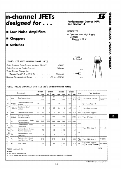
- Low Noise Amplifiers
- Operates from High Supply Voltages BVGSS>50V
| Part | 2N3684 |
|---|---|
| Description | n-channel JFET |
| Manufacturer | Siliconix |
| Size | 52.11 KB |
| Part Number | Manufacturer | Description |
|---|---|---|
| 2N3684 | Calogic LLC | N CHANNEL JFET LOW NOISE AMPLIFIER |
| 2N3684 | National Semiconductor | N-Channel JFETs |
| 2N3686 | National Semiconductor | N-Channel JFETs |
| 2N3685 | National Semiconductor | N-Channel JFETs |
| 2N3687 | National Semiconductor | N-Channel JFETs |