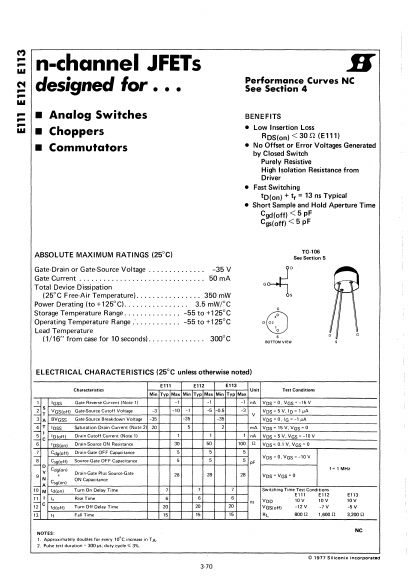
E111 Overview
Key Specifications
Mount Type: Panel
Length: 26 mm
Max Operating Temp: 65 °C
Min Operating Temp: -20 °C
Key Features
- C'? n-channel JFETs
- &II Choppers
| Part | E111 |
|---|---|
| Description | n-channel JFET |
| Manufacturer | Siliconix |
| Size | 63.84 KB |
Mount Type: Panel
Length: 26 mm
Max Operating Temp: 65 °C
Min Operating Temp: -20 °C
| Seller | Inventory | Price Breaks | Buy |
|---|---|---|---|
| Onlinecomponents.com | 195 | 5+ : 11.13 USD 25+ : 9.93 USD 50+ : 9.46 USD 100+ : 8.58 USD |
View Offer |
| DigiKey | 138 | 1+ : 12.91 USD 10+ : 10.969 USD 25+ : 10.282 USD 50+ : 9.7912 USD |
View Offer |
| Part Number | Manufacturer | Description |
|---|---|---|
| E1118 | ERG | Single Lamp DC to AC Inverter |
| M38B59MFH-E111FP | Mitsubishi Electric | 8-BIT SINGLE-CHIP MICROCOMPUTER |
| M38B59MFH-E111FP | Mitsubishi Electric | SINGLE-CHIP 8-BIT CMOS MICROCOMPUTER |
| E11FS3 | Nihon Inter Electronics | Fast Recovery Diode |
| E11W1 | ECLIPTEK | OSCILLATOR |