J1401
monolithic dual n-channel JFETs designed for
- -
- FEY Input Amplifiers
- - Low and Medium Frequency Amplifiers
- Impedance Converters
- Precision Instrumentation
Amplifiers
- parators
ABSOLUTE MAXIMUM RATINGS (25°C)
Gate-Drain or Gate-Source Voltage Forward Gate Current. Device Dissipation (each side)
@TA = 85°C derate 7.5 m Wr C
Total Device Dissipation
@TA = 85°C derate 11 m Wr C
Storage Temperature Range
50V l Orn A
300m W
500m W -55 to +150°C
Performance Curves NNR See Section 4
BENEFITS
- Low Cost
- Automatic I nsertion Package
- Symmetrical Pin-Out Allows Socket
Insertion in Either Direction
- Minimum System Error and Calibration
5 m V Offset Maximum (J1401)
95 d B Minimum CMRR (J1401-4)
- Operates from Low Power Supply Voltages
VGS(off) < 2_5V
- Simplifies Amplifier Design
Output Conductance < 2 Ilmho
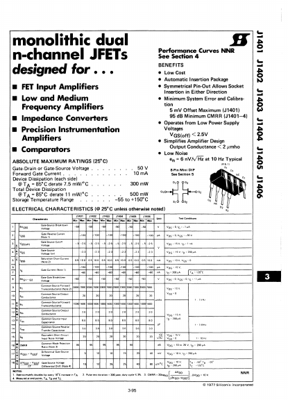
- Low Noise en = 6 n V/V'HZ at 10 Hz Typical a-Pin Mini DIP See Section 5
(PIN1) s,
D,
G,
~~...