Siliconix J1402
monolithic dual n-channel JFET
| Part No. | J1402 |
|---|---|
| Datasheet | J1402 Download |
| Manufacturer |  Siliconix |
| Description | monolithic dual n-channel JFET |
| Buy | Stock & Price |
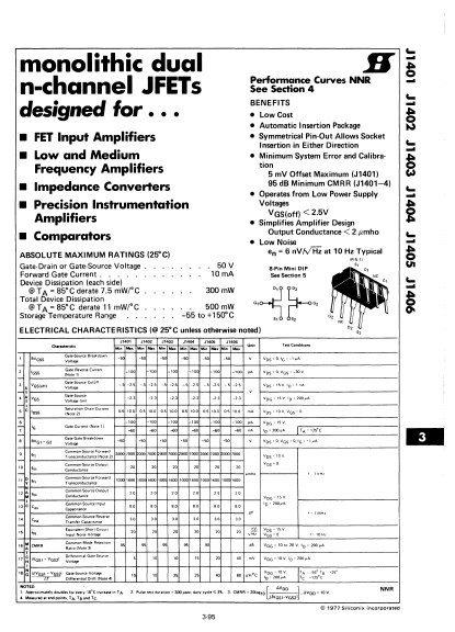
ABSOLUTE MAXIMUM RATINGS
(25°C) Gate-Drain or Gate-Source Voltage Forward Gate Current. Device Dissipation (each side) @TA = 85°C derate 7.5 mWrC Total Device Dissipation @TA = 85°C derate 11 mWrC Storage Temperature Range 50V lOrnA 300mW 500mW -55 to +150°C H Performance Curves NNR See Section 4 BENEFITS● Low Cost
● Automatic I nsertion Package
● Symmetrical Pin-Out Allows Socket Insertion in Either Direction
● Minimum System Error and Calibration 5 mV Offset Maximum (J1401) 95 dB Minimum CMRR (J1401-4)
● Operates from Low Power Supply Voltages VGS(off) < 2_5V
● Simplifies Amplifier Design Output Conductance < 2 Ilmho
● Low Noise en = 6 nV/V'HZ at 10 Hz Typical a-Pin Mini DIP See Section 5 (PIN1) s, D, G, ~~ G, G2 5, 52 G2 ""' -~ -""' -§ -""' B -g""'