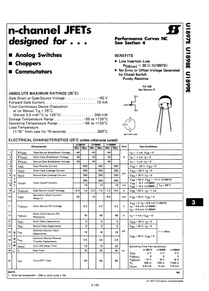
| Part | U1897E |
|---|---|
| Description | n-channel JFET |
| Manufacturer | Siliconix |
| Size | 65.47 KB |
Price & Availability
| Seller | Inventory | Price Breaks | Buy |
|---|---|---|---|
| No distributor offers were returned for this part. | |||
Related Datasheets
| Part Number | Manufacturer | Description |
|---|---|---|
| U1897 | Intersil | N-Channel JFET Switch |
| U1898 | Intersil | N-Channel JFET Switch |
| U1899 | Intersil | N-Channel JFET Switch |
| U1898 | Fairchild Semiconductor | N-Channel Switch |

