Click to expand full text
~Siliconix ~ im::orporated
VDDQ20
N-Channel Depletion-Mode MOSFET
DESIGNED FOR:
o Switching • Amplification
FEATURES
• High Breakdown Voltage> 200 V
• Low rOS(on) < 3 n
TYPE Single
PACKAGE
DEVICE
TO-206AC • ND2012E, ND2020E
TO-92 • ND2012L, ND2020L
Chip
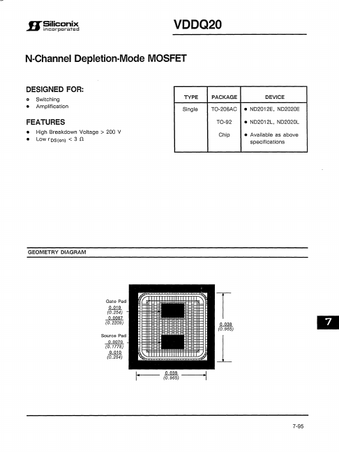
• Available as above specifications
GEOMETRY DIAGRAM
Gate Pad 0.010 (0.254) 0.0087
(0.2209)
Source Pad 0.0070
(0.1778) 0.010
(0.254)
T0.038
1 •(0.965)
7-95
VDDQ20
TYPICAL CHARACTERISTICS
~.-r-Sinicloircpoornatiexd
On-Resistance & Drain Current vs. Gate-Source Cutoff Voltage 25 r---~-----r----~----r----,1000
ros @ 10 = 20 rnA, VGS = 0 V
= =20 I----Ifo loss @ Vos 7.5 V, VGS 0 V 800
On-Resistance vs. Drain Current
::I~~tfIIIIIIV II ~IIIII
ros (.0. )
15 600 10
(rnA) 10 ~---4----~~~~----~--~400
rOS (.0.