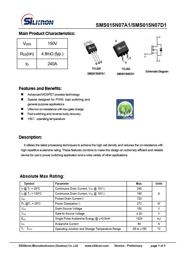
SMS015N07A1
SMS015N07A1 is MOSFET manufactured by Silikron.
Features and Benefits:
- Advanced MOSFET process technology
- Special designed for PWM, load switching and general purpose applications
- Ultra low on-resistance with low gate charge
- Fast switching and reverse body recovery
- 150℃ operating temperature
Description
:
It utilizes the latest processing techniques to achieve the high cell density and reduces the on-resistance with high repetitive avalanche rating. These features bine to make this design an extremely efficient and reliable device for use in power switching application and a wide variety of other applications.
Absolute Max Rating:
Symbol ID @ TC = 25°C ID @ TC = 100°C IDM PD @TC = 25°C VDS VGS EAS IAS TJ TSTG
Parameter Continuous Drain Current, VGS @ 10V① Continuous Drain Current, VGS @ 10V① Pulsed Drain Current② Power Dissipation③ Drain-Source Voltage Gate-to-Source Voltage Single Pulse Avalanche Energy @ L=0.5m H Avalanche Current Operating Junction and Storage Temperature Range
Max. 240 185 720 272 150 ± 20 1024 64 -55 to +150
Units
W V V m J A °C
©Silikron Microelectronics (Suzhou) Co.,Ltd
.silikron. Version : Preliminary page 1 of 5
Thermal Resistance
Symbol RθJC RθJA
Characteristics Junction-to-case ③ Junction-to-ambient ④
SMS015N07A1/SMS015N07D1
Typ.
- -
Max. 0.46 62
Units ℃/W
Electrical Characteristics @TA=25℃unless otherwise specified
Symbol V(BR)DSS RDS(on) VGS(th) IDSS
Parameter Drain-to-Source breakdown voltage Static Drain-to-Source on-resistance Gate threshold voltage Drain-to-Source leakage current Tj=25°C
IGSS
Gate-to-Source forward leakage
Qg
Total gate charge
Qgs
Gate-to-Source charge
Qgd
Gate-to-Drain("Miller") charge td(on)
Turn-on delay time tr
Rise time td(off)
Turn-Off delay time...