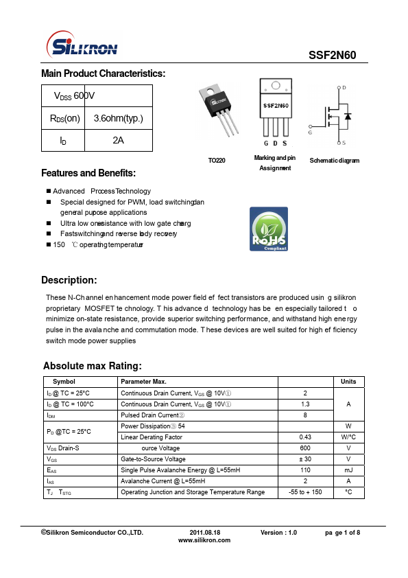
FEATURES AND BENEFITS
: Advanced Process Technology Special designed for PWM, load switching dan gene ral pur pose applications Ultra low on-r esistance with low gate charg e Fastswitching and re verse b ody reco very 150 ℃ operati ng temperatur e DESCRIPTION
: These N-Ch annel en hancement mode power field ef fect transistors are produced usin g silikron proprietary MOSFET te chnology. T his advance d technology has be en especially tailored t o minimize on-state resistance, provide superior switching performance, and withstand high ene rgy pulse in the avala nche and commutation mode. T hese devices are well suited for high ef ficiency switch mode power supplies Absolute max Rating: Symbol ID @ TC = 25°C ID @ TC = 100°C IDM PD @TC = 25°C VDS Drain-S VGS EAS IAS TJ TSTG Parameter Max. Continuous Drain Current, VGS @ 10V① Continuous Drain Current, VGS @ 10V① Pulsed Drain Current② Power Dissipation③ 54 Linear Derating Factor ource Voltage Gate-to-Source Voltage Single Pulse Aval... Silikron