SSFD6035U
Features
- Advanced MOSFET process technology
- Special design for PWM, load switching etc
- Ultra-low Rdson together with low gate charge
- Fast switch and body-diode trr
- 150℃ operating temperature
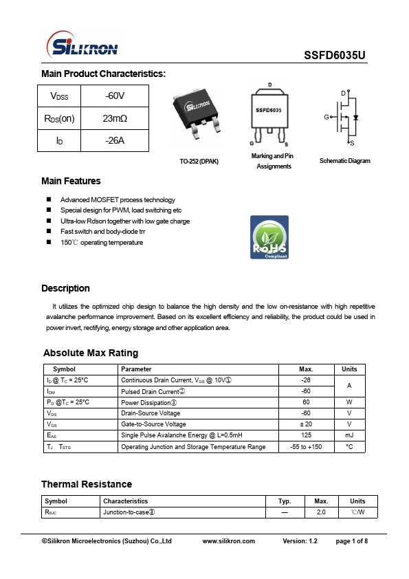
Marking and Pin Assignments
Schematic Diagram
Description
It utilizes the optimized chip design to balance the high density and the low on-resistance with high repetitive avalanche performance improvement. Based on its excellent efficiency and reliability, the product could be used in power invert, rectifying, energy storage and other application area.
Absolute Max Rating
Symbol ID @ TC = 25°C IDM PD @TC = 25°C VDS VGS EAS TJ TSTG
Parameter Continuous Drain Current, VGS @ 10V① Pulsed Drain Current② Power Dissipation③ Drain-Source Voltage Gate-to-Source Voltage Single Pulse Avalanche Energy @ L=0.5m H Operating Junction and Storage Temperature Range
Max. -26 -60 60 -60 ± 20 125 -55 to +150
Units
W V V m J °C
Thermal Resistance
Symbol RθJC
Characteristics...