SKY65120-21
SKY65120-21 is 2110-2170 MHz High Linearity / 2W Power Amplifier manufactured by Skyworks Solutions.
Features
- High linearity: OIP3 > +48 d Bm
- OP1d B = +33.5 d Bm
- ACLR =
- 45 d Bc for POUT = +25.4 d Bm
- High efficiency: PAE = 42%
- High gain = 24.6 d B
- Internal RF match and bias circuits
- Single DC supply: 5 V
- Small footprint, MCM (20-pin, 6 x 6 mm) SMT package (MSL3, 260 °C per JEDEC J-STD-020)
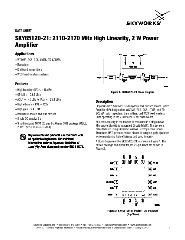
Figure 1. SKY65120-21 Block Diagram
Description
Skyworks SKY65120-21 is a fully-matched, surface mount Power Amplifier (PA) designed for WCDMA, PCS, DCS, UTMS, and TDSCDMA radio, repeaters, transmitters, and WCS fixed wireless units operating in the 2110 to 2170 MHz bandwidth. All active circuitry in the module is contained in a single Ga As Microwave Monolithic Integrated Circuit (MMIC). The device is manufactured using Skyworks Al Ga As Heterojunction Bipolar Transistor (HBT) process, which allows for single supply operation while maintaining high efficiency and good linearity. A block diagram of the SKY65120-21 is shown in Figure 1. The device package and pinout for the 20-pin MCM are shown in Figure 2.
Figure 2. SKY65120-21 Pinout
- 20-Pin MCM (Top View)
Skyworks Solutions, Inc.
- Phone [781] 376-3000
- Fax [781] 376-3100
- sales@skyworksinc.
- .skyworksinc.
200816E
- Skyworks Proprietary Information
- Products and Product Information are Subject to Change Without Notice
- January 13, 2012 1
Free Datasheet http://.n Datasheet.
DATA SHEET
- SKY65120-21 2110-2170 MHZ HIGH LINEARITY PA
Table 1. SKY65120-21 Signal Descriptions
Pin # 1 2 3 4 5 6 7 8 9 10
Note:
Name GND GND GND VC_BIAS N/C VREF1 VREF2 GND RF_OUT GND Ground Ground Ground Bias voltage No connection
Description
Pin # 11 12 13 14 15 16 17 18 19 20 VCC2 N/C VCC1 N/C N/C RF_IN GND N/C GND GND
Name No connection
Description
Stage 2 collector voltage Stage 1 collector voltage No connection No connection RF input Ground No connection Ground Ground
Bias reference voltage 1 Bias reference voltage 2 Ground RF output Ground
The center ground pad must have a low inductance and low thermal resistance...