SL11P06D
SL11P06D is P-CHANNEL MOSFET manufactured by Slkor Micro Semicon.
Features
- VDS =-60V,ID =-11A RDS(ON) <180 mΩ @ VGS=-10V RDS(ON) <220 mΩ @ VGS=-4.5V
- Improved dv/dt capability
- Fast switching
- Good stability and uniformity with high EAS
- Excellent package for good heat dissipation
Applications
- Power switching application
- Hard switched and high frequency circuits
- LED Lighting
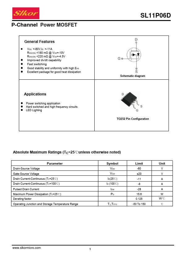
Schematic diagram TO252 Pin Configuration
Absolute Maximum Ratings (TC=25℃unless otherwise noted)
Drain-Source Voltage
Parameter
Gate-Source Voltage
Drain Current-Continuous (TC=25℃) Drain Current-Continuous (TC=100℃)
Pulsed Drain Current Maximum Power Dissipation (TC=25℃) Derating factor
Operating Junction and Storage Temperature Range
Symbol VDS VGS
ID(25℃)
ID (100℃)
IDM PD
TJ,TSTG
Limit
-60 ±20 -11 -8 -28 15.6 0.125 -50 To 150
Unit
V V A A A W W/℃ ℃
.slkormicro.
Thermal Characteristic
Thermal Resistance,Junction-to-Case(Note 2)
RθJC
Electrical Characteristics (TC=25℃unless otherwise noted)
℃/W
Parameter
Off Characteristics Drain-Source Breakdown Voltage Zero Gate Voltage Drain Current Gate-Body Leakage Current On Characteristics (Note 3) Gate Threshold Voltage
Drain-Source On-State Resistance
Forward Transconductance Dynamic Characteristics (Note4) Input Capacitance Output Capacitance Reverse Transfer Capacitance Switching Characteristics (Note 4) Turn-on Delay Time Turn-on Rise Time Turn-Off Delay Time Turn-Off Fall Time Total Gate Charge
Gate-Source Charge
Gate-Drain Charge Drain-Source Diode Characteristics Diode Forward Voltage (Note 3) Diode Forward Current (Note 2) Forward Turn-On...