Datasheet4U Logo Datasheet4U.com

CXL5514M - CMOS-CCD 1H Delay Line for PAL

Datasheet Summary

Description

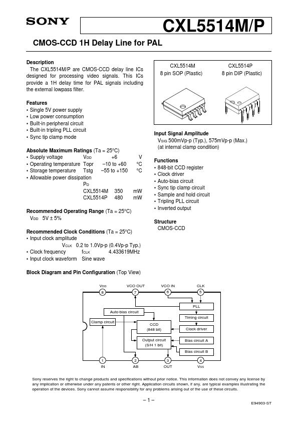
The CXL5514M/P are CMOS-CCD delay line ICs designed for processing video signals.

This ICs provide a 1H delay time for PAL signals including the external lowpass filter.

Features

  • Single 5V power supply.
  • Low power consumption.
  • Built-in peripheral circuit.
  • Built-in tripling PLL circuit.
  • Sync tip clamp mode Absolute Maximum Ratings (Ta = 25°C).
  • Supply voltage VDD +6.
  • Operating temperature Topr.
  • 10 to +60.
  • Storage temperature Tstg.
  • 55 to +150.
  • Allowable power dissipation PD CXL5514M 350 CXL5514P 480 Recommended Operating Range (Ta = 25°C) VDD 5V ± 5% Recommended Clock Conditions.

📥 Download Datasheet

Datasheet preview – CXL5514M

Datasheet Details

Part number CXL5514M
Manufacturer Sony Corporation
File Size 143.76 KB
Description CMOS-CCD 1H Delay Line for PAL
Datasheet download datasheet CXL5514M Datasheet
Additional preview pages of the CXL5514M datasheet.
Other Datasheets by Sony Corporation

Full PDF Text Transcription

Click to expand full text
CXL5514M/P CMOS-CCD 1H Delay Line for PAL Description The CXL5514M/P are CMOS-CCD delay line ICs designed for processing video signals. This ICs provide a 1H delay time for PAL signals including the external lowpass filter. Features • Single 5V power supply • Low power consumption • Built-in peripheral circuit • Built-in tripling PLL circuit • Sync tip clamp mode Absolute Maximum Ratings (Ta = 25°C) • Supply voltage VDD +6 • Operating temperature Topr –10 to +60 • Storage temperature Tstg –55 to +150 • Allowable power dissipation PD CXL5514M 350 CXL5514P 480 Recommended Operating Range (Ta = 25°C) VDD 5V ± 5% Recommended Clock Conditions (Ta = 25°C) • Input clock amplitude VCLK 0.2 to 1.0Vp-p (0.4Vp-p Typ.) • Clock frequency fCLK 4.
Published: |