CXL5515P
CXL5515P is CMOS-CCD 1H Delay Line for PAL manufactured by Sony Semiconductor Solutions.
CXL5515M/P
CMOS-CCD 1H Delay Line for PAL
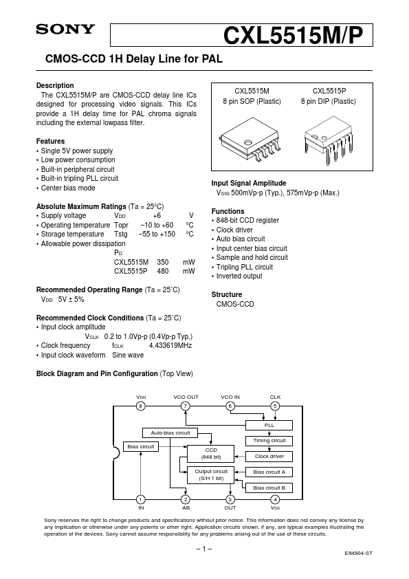
Description The CXL5515M/P are CMOS-CCD delay line ICs designed for processing video signals. This ICs provide a 1H delay time for PAL chroma signals including the external lowpass filter. Features
- Single 5V power supply
- Low power consumption
- Built-in peripheral circuit
- Built-in tripling PLL circuit
- Center bias mode...