SSM4953
SSM4953 is Dual P-Channel MOSFET manufactured by South Sea Semiconductor.
Dual P-Channel Enhancement Mode MOSFET
Product Summary
VDS (V)
-30V
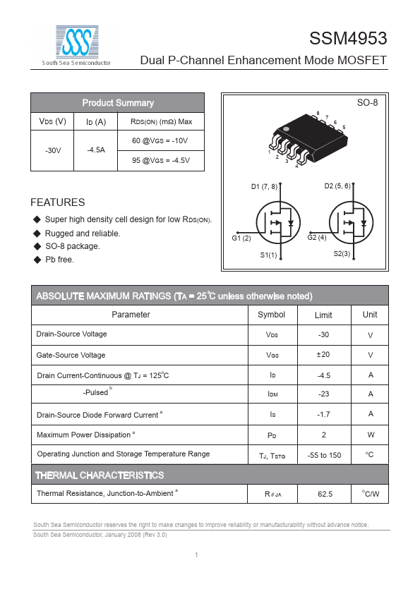
SO-8
8 7 6 5
ID (A)
-4.5A
RDS(ON) (mΩ) Max 60 @VGS = -10V
95 @VGS = -4.5V
D1 (7, 8)
D2 (5, 6)
Features
Super high density cell design for low R DS(ON). Rugged and reliable. SO-8 package. Pb free.
G1 (2) S1(1) G2 (4)...