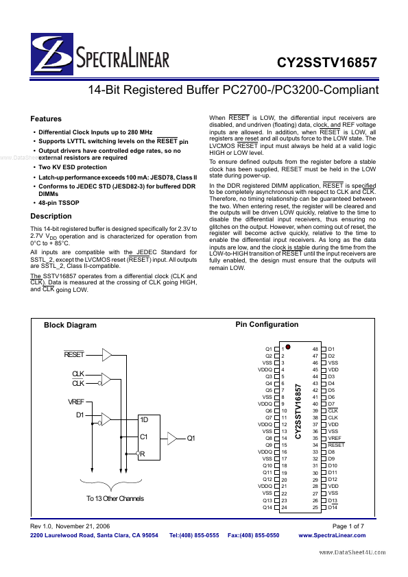
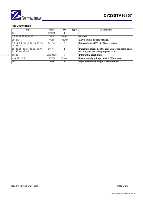
Datasheet4U Logo Datasheet4U.com

CY2SSTV16857 - 14-Bit Regstered Buffer

Datasheet Summary

Description

This 14-bit registered buffer is designed specifically for 2.3V to 2.7V VDD operation and is characterized for operation from 0°C to + 85°C.

All inputs are compatible with the JEDEC Standard for SSTL_2, except the LVCMOS reset (RESET) input.

All outputs are SSTL_2, Class II-compatible.

Features

  • Differential Clock Inputs up to 280 MHz.
  • Supports LVTTL switching levels on the RESET pin.
  • Output drivers have controlled edge rates, so no www. DataSheet4U. com external resistors are required.
  • Two KV ESD protection.
  • Latch-up performance exceeds 100 mA: JESD78, Class II.
  • Conforms to JEDEC STD (JESD82-3) for buffered DDR DIMMs.
  • 48-pin TSSOP When RESET is LOW, the differential input receivers are disabled, and undriven (floating) data,.

📥 Download Datasheet

Datasheet preview – CY2SSTV16857

Datasheet Details

Part number CY2SSTV16857
Manufacturer SpectraLinear
File Size 125.53 KB
Description 14-Bit Regstered Buffer
Datasheet download datasheet CY2SSTV16857 Datasheet
Additional preview pages of the CY2SSTV16857 datasheet.
Other Datasheets by SpectraLinear

Full PDF Text Transcription

Click to expand full text
CY2SSTV16857 14-Bit Registered Buffer PC2700-/PC3200-Compliant Features • Differential Clock Inputs up to 280 MHz • Supports LVTTL switching levels on the RESET pin • Output drivers have controlled edge rates, so no www.DataSheet4U.com external resistors are required • Two KV ESD protection • Latch-up performance exceeds 100 mA: JESD78, Class II • Conforms to JEDEC STD (JESD82-3) for buffered DDR DIMMs • 48-pin TSSOP When RESET is LOW, the differential input receivers are disabled, and undriven (floating) data, clock, and REF voltage inputs are allowed. In addition, when RESET is LOW, all registers are reset and all outputs force to the LOW state. The LVCMOS RESET input must always be held at a valid logic HIGH or LOW level.
Published: |