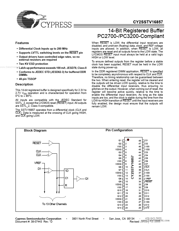
CY2SSTV16857 Key Features
- Differential Clock Inputs up to 280 MHz
- Supports LVTTL switching levels on the RESET pin
- Output drivers have controlled edge rates, so no external resistors are required
- Two KV ESD protection
- Latch-up performance exceeds 100 mA: JESD78, Class II
- Conforms to JEDEC STD (JESD82-3) for buffered DDR DIMMs
- 48-pin TSSOP