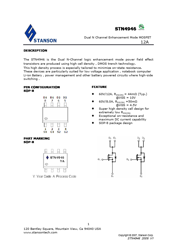
DESCRIPTION
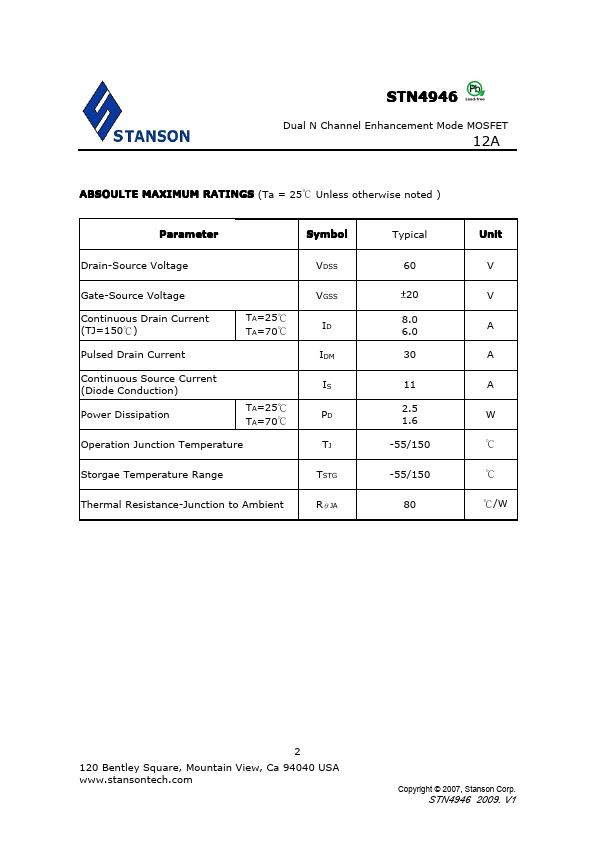
PIN CONFIGURATION SOP-8 FEATURE 60V/12A, RDS(ON) = 44mΩ (Typ.) @VGS = 10V 60V/8.0A, RDS(ON) =50mΩ @VGS = 4.5V Super high density cell design for extremely low RDS(ON) Exceptional on-resistance and maximum DC current capability SOP-8 package design PART MARKING SOP-8 1 120 Bentley Square, Mountain View, Ca 94040 USA Copyright © 2007, Stanson Corp. STN4946 2009. V1 STN4946 Dual N Channel Enhancement Mode MOSFET 12A ABSOULTE MAXIMUM RATINGS
(Ta = 25℃ Unless otherwise noted ) Parameter Symbol Drain-Source Voltage VDSS Gate-Source Voltage Continuous Drain Current (TJ=150℃) TA=25℃ TA=70℃ Pulsed Drain Current Continuous Source Current (Diode Conduction) Power Dissipation TA=25℃ TA=70℃ Operation Junction Temperature VGSS ID IDM IS PD TJ Storgae Temperature Range Thermal Resistance-Junction to Ambient TSTG RθJA Typical 60 ±20 8.0 6.0 30 11 2.5 1.6 -55/150 -55/150 80 Unit V V A A A W ℃ ℃ ℃/W 2 120 Bentley Square, Mountain View, Ca 94040 USA Copyright © 2007, Stanson Corp. STN4946 2009. Stanson Technology