FEATURES
❏ HVCMOS® technology ❏ Operating output voltage of 240V ❏ Low power level shifting from 5V to 240V ❏ Shift register speed 8MHz @ VDD = 5V ❏ 12 latched data outputs ❏ Output polarity and blanking ❏ CMOS compatible inputs ❏ Forward and reverse shifting options GENERAL DESCRIPTION
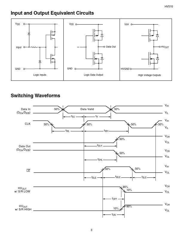
The device consists of a 12-bit shift register, 12 latches, and control logic to perform the polarity select and blanking of the outputs. A DIR pin controls the direction of data shift through the device. With DIR grounded, DIOA is Data In and DIOB is Data Out; data is shifted from HVOUT12 to HVOUT1. When DIR is at logic high, DIOB is Data In and DIOA is Data Out: data is then shifted from HVOUT1 to HVOUT12. Data is shifted through the shift register on the low to high transition of the clock. Data output buffers are provided for cascading devices. Operation of the shift register is not affected by the LE, BL, or the POL inputs. Transfer of data from the shift register to the latch occurs when the LE is high. Supertex Inc