FEATURES
XXHVCMOS® technology for high performance XXVery low quiescent power dissipation (-10µA max.) XXOutput on-resistance typically (22Ω typ.) XXIntegrated bleed resistors on the outputs XXLow parasitic capacitances ►►DC to 50MHz small signal frequency response XX-60dB typical output OFF isolation at 5.0MHz XXCMOS logic circuitry for low power XXExcellent noise immunity XXON-chip shift register, latch and clear logic circuitry XXFlexible high voltage supplies APPLICATIONS
XX Medical ultrasound imaging XX Piezoelectric transducer drivers GENERAL DESCRIPTION
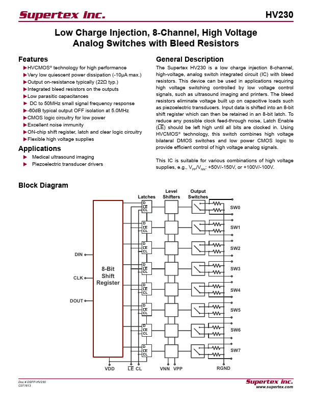
The Supertex Input data is shifted into an 8-bit shift register which can then be retained in an 8-bit latch. To reduce any possible clock feed-through noise, Latch Enable (LE) should be left high until all bits are clocked in. Using HVCMOS® technology, this switch combines high voltage bilateral DMOS switches and low power CMOS logic to provide efficient control of high voltage analog signals. This IC is suitable for various combinations of high voltage supplies, e.g., VPP/VNN: +50V/-150V, or +100V/-100V. Supertex