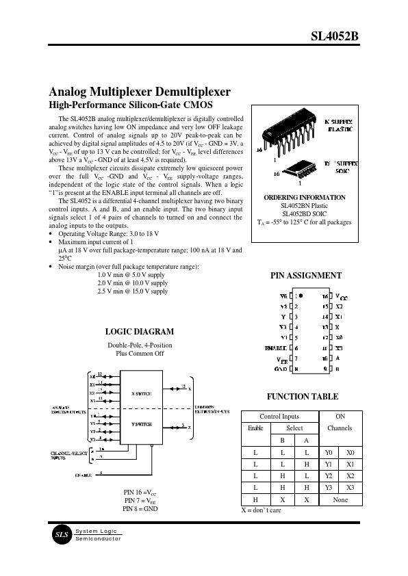
• Part: SL4052B
  • Description: Analog Multiplexer Demultiplexer High-Performance Silicon-Gate CMOS
  • Manufacturer: System Logic Semiconductor
  • Size: 61.29 KB
Download SL4052B Datasheet PDF
System Logic Semiconductor
SL4052B
SL4052B is Analog Multiplexer Demultiplexer High-Performance Silicon-Gate CMOS manufactured by System Logic Semiconductor.
Analog Multiplexer Demultiplexer High-Performance Silicon-Gate CMOS The SL4052B analog multiplexer/demultiplexer is digitally controlled analog switches having low ON impedance and very low OFF leakage current. Control of analog signals up to 20V peak-to-peak can be achieved by digital signal amplitudes of 4.5 to 20V (if VCC - GND = 3V, a VCC - VEE of up to 13 V can be controlled; for VCC - VEE level differences above 13V a VCC - GND of at least 4.5V is required). These multiplexer circuits dissipate extremely low quiescent power over the full VCC -GND and VCC - VEE supply-voltage ranges, independent of the logic state of the control signals. When a logic “1”is present at the ENABLE input terminal all channels are off. The SL4052 is a differential 4-channel multiplexer having two binary control inputs. A and B, and an enable input. The two binary input signals select 1 of 4 pairs of channels to turned on and connect the analog inputs to the outputs. - Operating Voltage Range: 3.0 to 18 V - Maximum input current of 1 µA at 18 V over full package-temperature range; 100 n A at 18 V and 25°C - Noise margin (over full package temperature range): 1.0 V min @ 5.0 V supply 2.0 V min @ 10.0 V supply 2.5 V min @ 15.0 V supply ORDERING INFORMATION SL4052BN Plastic SL4052BD SOIC TA = -55° to 125° C for all packages PIN ASSIGNMENT LOGIC DIAGRAM Double-Pole, 4-Position Plus mon Off FUNCTION TABLE Control Inputs Enable B L L L PIN 16 =VCC PIN 7 = VEE PIN 8 = GND System Logic Semiconductor ON Channels A L H L H X Y0 Y1 Y2 Y3 X0 X1 X2 X3 None Select L L H H X X = don’t care MAXIMUM RATINGS - Symbol VCC VIN VOUT IIN PD PD Tstg TL - Parameter DC Supply Voltage (Referenced to GND) DC Input Voltage (Referenced to GND) DC Output Voltage (Referenced to GND) DC Input Current, per Pin Power Dissipation in Still Air, Plastic DIP+ SOIC Package+ Power Dissipation per Output Transistor Storage Temperature Lead Temperature, 1 mm from Case for 10 Seconds...