SL74LVU04
SL74LVU04 is Hex Inverter manufactured by System Logic Semiconductor.
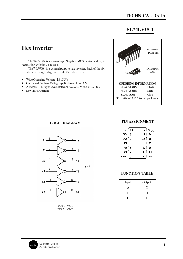
TECHNICAL DATA
Hex Inverter
The 74LVU04 is a low-voltage, Si-gate CMOS device and is pin patible with the 74HCU04. The 74LVU04 is a general purpose hex inverter. Each of the six inverters is a single stage with unbuffered outputs.
- -
- - Wide Operating Voltage: 1.0÷5.5 V Optimized for Low Voltage applications: 1.0÷3.6 V Accepts TTL input levels between VCC =2.7 V and VCC =3.6 V Low Input Current
14 1 14 1
N SUFFIX PLASTIC
D SUFFIX SOIC
ORDERING INFORMATION SL74LVU04N Plastic SL74LVU04D SOIC SL74LVU04 Chip TA = -40° ÷ 125° C for all packages
LOGIC DIAGRAM
PIN ASSIGNMENT
FUNCTION TABLE
Input A L H PIN 14 =VCC PIN 7 = GND Output Y H L
System Logic Semiconductor
MAXIMUM RATINGS
- Symbol VCC IIK
- 1 2
Parameter DC supply voltage (Referenced to GND) DC input diode current DC output diode current DC output source or sink current -bus driver outputs DC VCC current for types with
- bus driver outputs DC GND current for types with
- bus driver outputs Power dissipation per package, plastic DIP+ SOIC package+ Storage temperature Lead temperature, 1.5 mm from Case for 10 seconds (Plastic DIP ), 0.3 mm (SOIC Package)
Value -0.5 ÷ +7.0 ±20 ±50 ±25 ±50 ±50 750 500 -65 ÷ +150 260
Unit V m A m A m A m A m A m W °C °C
- IO
- ICC IGND PD
Tstg TL
- Maximum Ratings are those values beyond which damage to the device may occur. Functional operation should be restricted to the Remended Operating Conditions. +Derating
- Plastic DIP:
- 12 m W/°C from 70° to 125°C SOIC Package: :
- 8 m W/°C from 70° to 125°C
- 1: VI < -0.5V or VI > VCC+0.5V
- 2: Vo < -0.5V or Vo > VCC+0.5V
- 3: -0.5V < Vo < VCC+0.5V
REMENDED OPERATING CONDITIONS
Symbol VCC VIN, VOUT TA tr, t f Parameter DC Supply Voltage (Referenced to GND) DC Input Voltage, Output Voltage (Referenced to GND) Operating Temperature, All Package Types Input Rise and Fall Time 1.0 V≤VCC <2.0 V 2.0 V≤VCC <2.7 V 2.7 V≤VCC <3.6 V 3.6 V≤VCC ≤5.5 V Min 1.0 0 -40 0 0 0 0 Max 5.5 VCC +125 500 200 100 50...