DESCRIPTION
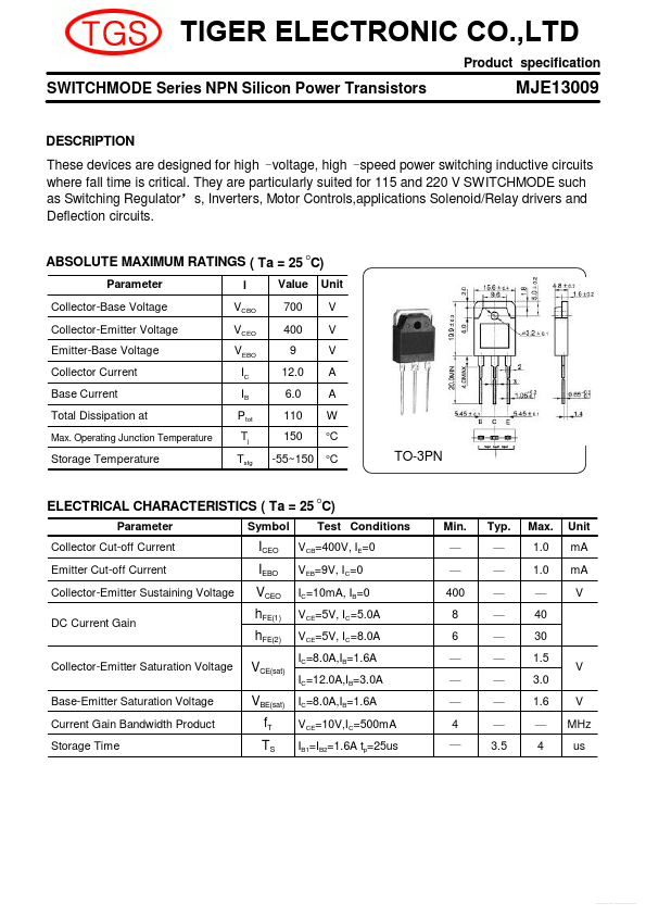
These devices are designed for high–voltage, high–speed power switching inductive circuits where fall time is critical. They are particularly suited for 115 and 220 V SWITCHMODE such as Switching Regulator’s, Inverters, Motor Controls,applications Solenoid/Relay drivers and Deflection circuits. O ABSOLUTE MAXIMUM RATINGS
( Ta = 25 C) Parameter Collector-Base Voltage Collector-Emitter Voltage Emitter-Base Voltage Collector Current Base Current Total Dissipation at Max. Operating Junction Temperature l VCBO VCEO VEBO IC IB Ptot Tj Tstg Value 700 400 9 12.0 6.0 110 150 -55~150 Unit V V V A A W o o C C Storage Temperature TO-3PN ELECTRICAL CHARACTERISTICS
( Ta = 25 C) Parameter Collector Cut-off Current Emitter Cut-off Current Collector-Emitter Sustaining Voltage DC Current Gain Symbol Test Conditions VCB=400V, IE=0 VEB=9V, IC=0 IC=10mA, IB=0 VCE=5V, IC=5.0A VCE=5V, IC=8.0A IC=8.0A,IB=1.6A IC=12.0A,IB=3.0A Base-Emitter Saturation Voltage Current Gain Bandwidth Product Storage Time Min. — — 400 8 6 — — — 4 — Typ. — — — — — — — — — 3.5 Max. TGS