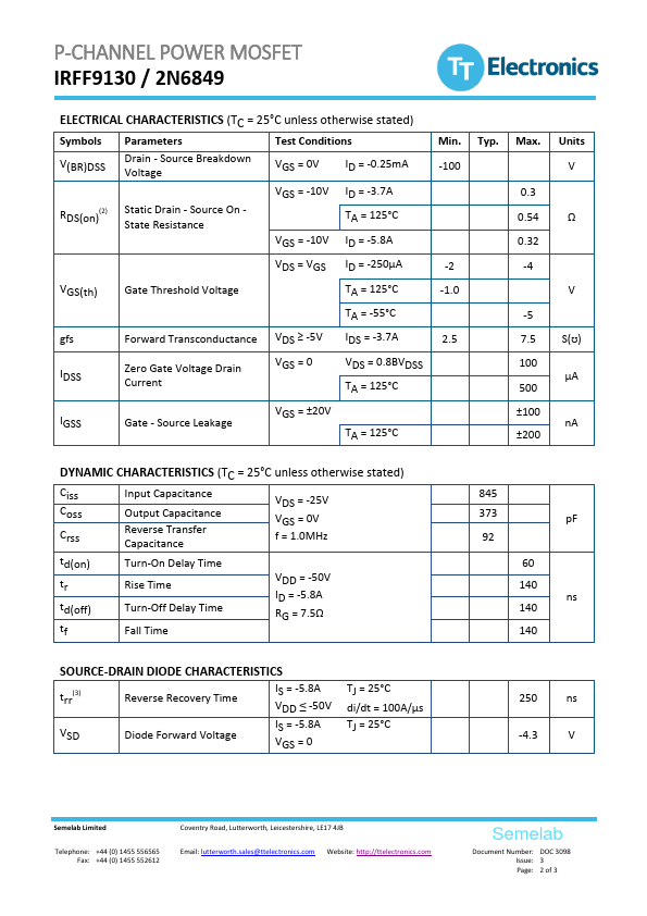
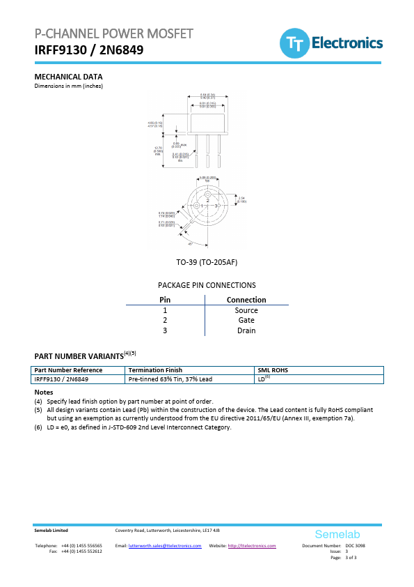
TT 2N6849
P-CHANNEL POWER MOSFET
| Part No. | 2N6849 |
|---|---|
| Datasheet | 2N6849 Download |
| Manufacturer |  TT |
| Description | P-CHANNEL POWER MOSFET |
| Buy | Stock & Price |
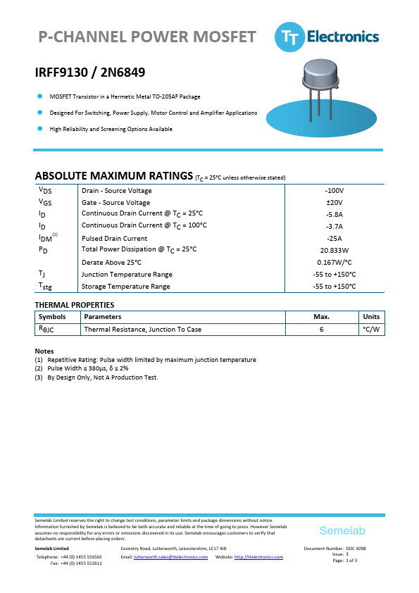
APPLICATIONS
High Reliability and Screening Options AvailableABSOLUTE MAXIMUM RATINGS
(TC = 25°C unless otherwise stated) VDS Drain - Source Voltage VGS Gate - Source Voltage ID Continuous Drain Current @ TC = 25°C ID IDM(1) Continuous Drain Current @ TC = 100°C Pulsed Drain Current PD Total Power Dissipation @ TC = 25°C Derate Above 25°C TJ Junction Temperature Range Tstg Storage Temperature Range THERMAL PROPERTIES Symbols Parameters RθJC Thermal Resistance, Junction To Case Notes (1) Repetitive Rating: Pulse width limited by maximum junction temperature (2) Pulse Width ≤ 380µs, δ ≤ 2% (3) By Design Only, Not A Production Test. -100V ±20V -5.8A -3.7A -25A 20.833W 0.167W/°C -55 to +150°C -55 to +150°C Max. 6 Units °C/W Semelab Limited reserves the right to change test conditions, parameter limits and package dimensions without notice. Information furnished by Semelab is believed to be both accurate and reliable at the time of going to press. However Semelab assumes no responsibility for any errors or omissions discovered in its use.