TT D2014UK
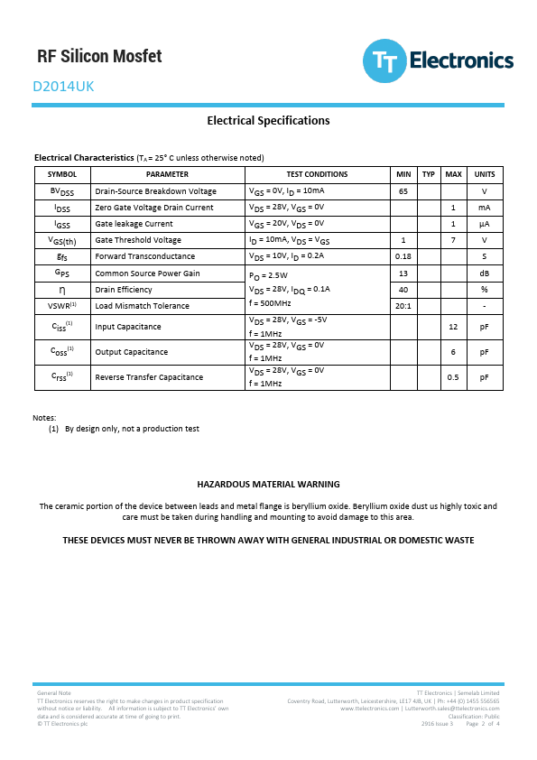
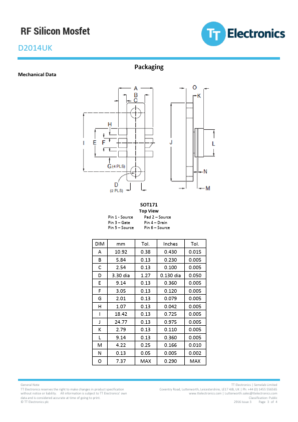
The ceramic portion of the device between leads and metal flange is beryllium oxide.| Part No. | D2014UK |
|---|---|
| Datasheet | D2014UK Download |
| Manufacturer |  TT |
| Description | RF Silicon Mosfet |
| Buy | Stock & Price |
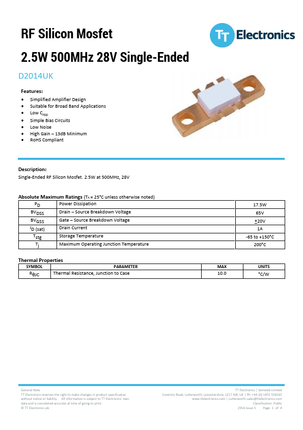
FEATURES
:● Simplified Amplifier Design
● Suitable for Broad Band
APPLICATIONS
● Low Crss● Simple Bias Circuits
● Low Noise
● High Gain – 13dB Minimum
● RoHS Compliant
DESCRIPTION
: Single-Ended RF Silicon Mosfet. 2.5W at 500MHz, 28VABSOLUTE MAXIMUM RATINGS
(TA = 25°C unless otherwise noted) PD Power Dissipation BVDSS Drain – Source Breakdown Voltage BVGSS Gate – Source Breakdown Voltage ID (sat) Drain Current Tstg Storage Temperature Tj Maximum Operating Junction Temperature Thermal Properties SYMBOL PARAMETER RθJC Thermal Resistance, Junction to Case 17.5W 65V +20V 1A -65 to +150°C 200°C MAX UNITS 10.0 °C/W General Note TT Electronics reserves the right to make changes in product specification without notice or liability. All information is subject to TT Electronics’ own data and is considered accurate at time of going to print. © TT Electronics plc TT Electronics | Semelab Limited Coventry Road, Lutterworth, Leicestershire, LE17 4JB, UK | Ph: +44 (0) 1455 556565 | Lutterworth.sales...