TSM10N80CI Overview
Description
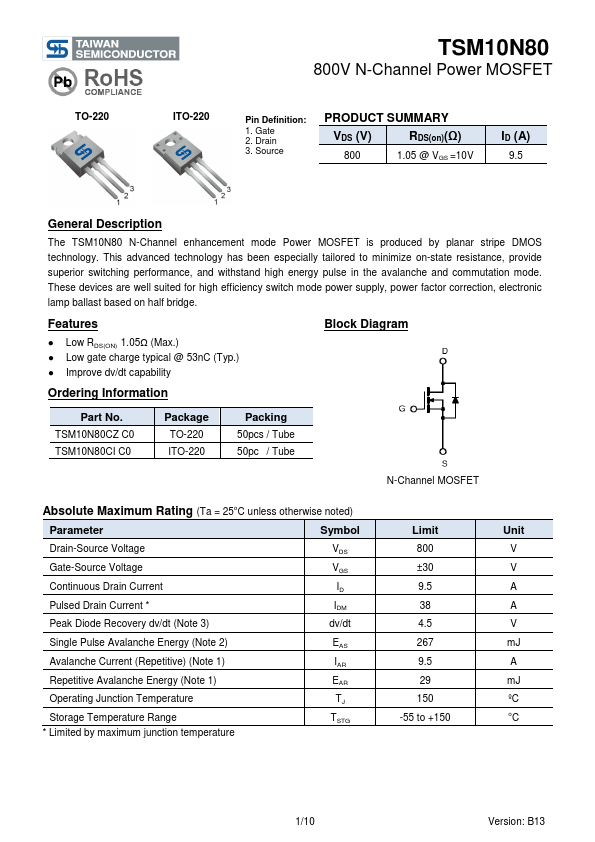
The TSM10N80 N-Channel enhancement mode Power MOSFET is produced by planar stripe DMOS technology. This advanced technology has been especially tailored to minimize on-state resistance, provide superior switching performance, and withstand high energy pulse in the avalanche and commutation mode.
Key Features
- Low RDS(ON) 1.05Ω (Max.) Low gate charge typical @ 53nC (Typ.) Improve dv/dt capability