Taiwan Semiconductor TSM3442
20V N-CHANNEL MOSFET
| Part No. | TSM3442 |
|---|---|
| Datasheet | TSM3442 Download |
| Manufacturer |  Taiwan Semiconductor |
| Description | 20V N-CHANNEL MOSFET |
| Buy | Stock & Price |
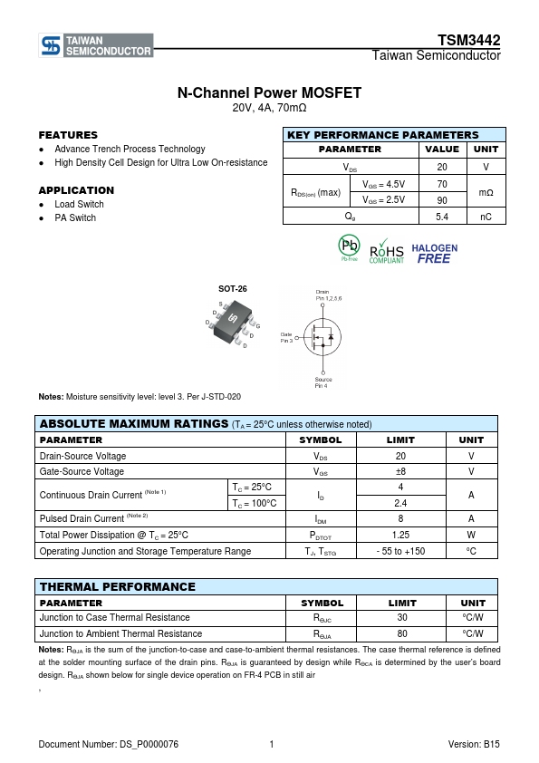
FEATURES
● Advance Trench Process Technology● High Density Cell Design for Ultra Low On-resistance APPLICATION
● Load Switch
● PA Switch KEY PERFORMANCE PARAMETERS PARAMETER VALUE UNIT VDS 20 V VGS = 4.5V 70 RDS(on) (max) VGS = 2.5V 90 mΩ Qg 5.4 nC SOT-26 Notes: Moisture sensitivity level: level 3. Per J-STD-020
ABSOLUTE MAXIMUM RATINGS
(TA = 25°C unless otherwise noted) PARAMETER SYMBOL LIMIT Drain-Source Voltage Gate-Source Voltage Continuous Drain Current (Note 1) Pulsed Drain Current (Note 2) TC = 25°C TC = 100°C Total Power Dissipation @ TC = 25°C Operating Junction and Storage Temperature Range VDS VGS ID IDM PDTOT TJ, TSTG 20 ±8 4 2.4 8 1.25 - 55 to +150 UNIT V V A A W °CTHERMAL PERFORMANCE
PARAMETER SYMBOL LIMIT UNIT Junction to Case Thermal Resistance RӨJC 30 °C/W Junction to Ambient Thermal Resistance RӨJA 80 °C/W Notes: RӨJA is the sum of the junction-to-case and case-to-ambient thermal resistances. The case thermal reference is defined at the solder mounting surface of the drain pins.