Taiwan Semiconductor TSM3443
The products shown herein are not designed for use in medical, life-saving, or life-sustaining applications.| Part No. | TSM3443 |
|---|---|
| Datasheet | TSM3443 Download |
| Manufacturer |  Taiwan Semiconductor |
| Description | 20V P-CHANNEL MOSFET |
| Buy | Stock & Price |
FEATURES
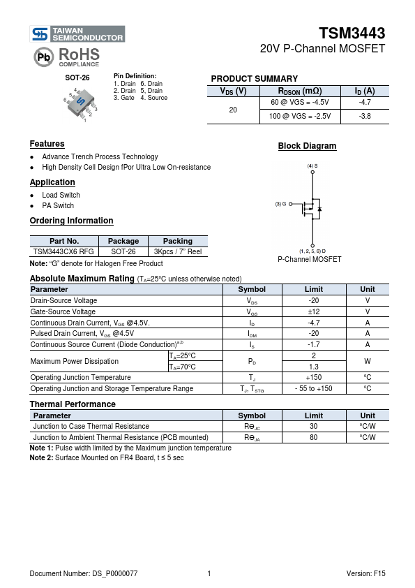
● Advance Trench Process Technology● High Density Cell Design fPor Ultra Low On-resistance Application
● Load Switch
● PA Switch Ordering Information Block Diagram Part No. Package Packing TSM3443CX6 RF SOT-26 3Kpcs / 7” Reel TSM3443CX6 RFG SOT-26 3Kpcs / 7” Reel Note: “G” denote for Halogen Free Product
ABSOLUTE MAXIMUM RATINGS
(TA=25oC unless otherwise noted) Parameter Symbol Drain-Source Voltage Gate-Source Voltage Continuous Drain Current, VGS @4.5V. Pulsed Drain Current, VGS @4.5V Continuous Source Current (Diode Conduction)a,b Maximum Power Dissipation TA=25oC TA=70oC Operating Junction Temperature Operating Junction and Storage Temperature Range VDS VGS ID IDM IS PD TJ TJ, TSTGTHERMAL PERFORMANCE
Parameter Junction to Case Thermal Resistance Junction to Ambient Thermal Resistance (PCB mounted) Note 1: Pulse width limited by the Maximum junction temperature Note 2: Surface Mounted on FR4 Board, t ≤ 5 sec Symbol RӨJC RӨJA P-Channel MOSFET Limit -20 ±12 -4.7 -20 -1.7 2 1...