TSM35N10
Features
- -
- - Advanced Trench Technology Low RDS(ON) 37mΩ (Max.) Low gate charge typical @ 34n C (Typ.) Low Crss typical @ 45p F (Typ.)
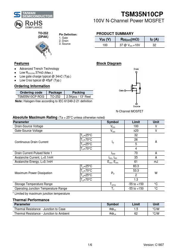
Block Diagram
Ordering Information
Part No.
TSM35N10CP ROG
Package
TO-252
Packing
2.5Kpcs / 13” Reel
Note: “G” denote for Halogen Free Product N-Channel MOSFET
Absolute Maximum Rating (Ta = 25o C unless otherwise noted)
Parameter
Drain-Source Voltage Gate-Source Voltage TC=25° C TC=70° C TA=25° C TA=70° C
Symbol
VDS VGS
Limit
100 ±20 32 26 5 4 70 35 61 83.3 53.3 2 1.3 -55 to +150 -55 to +150
Unit
Continuous Drain Current
Drain Current-Pulsed Note 1 Avalanche Current, L=0.1m H Avalanche Energy, L=0.1m H TC=25° C Maximum Power Dissipation TC=70° C TA=25° C TA=70° C
IDM IAS, IAR EAS, EAR
A A m J
Storage Temperature Range Operating Junction Temperature Range
- Limited by maximum junction temperature
TSTG TJ
° C ° C
Thermal Performance
Parameter
Thermal Resistance
- Junction to Case Thermal Resistance
- Junction to...