Taiwan Semiconductor TSM4433D
The products shown herein are not designed for use in medical, life-saving, or life-sustaining appl| Part No. | TSM4433D |
|---|---|
| Datasheet | TSM4433D Download |
| Manufacturer |  Taiwan Semiconductor |
| Description | 20V Dual P-Channel MOSFET |
| Buy | Stock & Price |
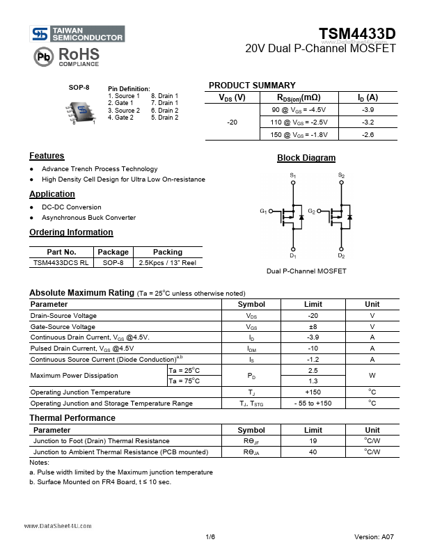
FEATURES
●● Advance Trench Process Technology High Density Cell Design for Ultra Low On-resistance Block Diagram Application
●
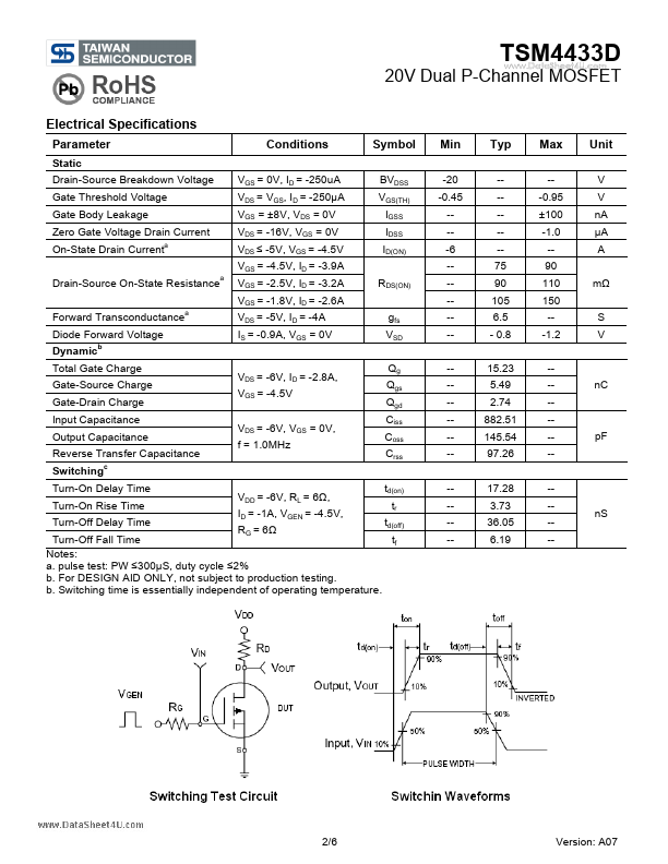
● DC-DC Conversion Asynchronous Buck Converter Ordering Information Part No. TSM4433DCS RL Package SOP-8 Packing 2.5Kpcs / 13” Reel Dual P-Channel MOSFET Absolute Maximum Rating (Ta = 25oC unless otherwise noted) Parameter Drain-Source Voltage Gate-Source Voltage Continuous Drain Current, VGS @4.5V. Pulsed Drain Current, VGS @4.5V Continuous Source Current (Diode Conduction) Maximum Power Dissipation Operating Junction Temperature Operating Junction and Storage Temperature Range a,b o o Symbol VDS VGS ID IDM IS PD TJ TJ, TSTG Ta = 25 C Ta = 75 C Limit -20 ±8 -3.9 -10 -1.2 2.5 1.3 +150 - 55 to +150 Unit V V A A A W o o C C
THERMAL PERFORMANCE
Parameter Junction to Foot (Drain) Thermal Resistance Junction to Ambient Thermal Resistance (PCB mounted) Notes: a. Pulse width limited by the Maximum junction temperature b. Surface Mounted on FR4 Board, t ≤ 10 sec. Symb...