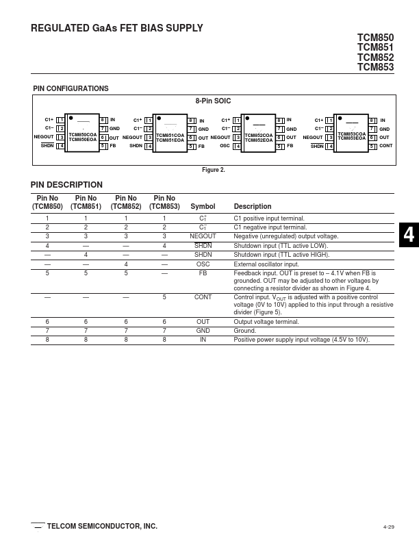
TCM851 Description
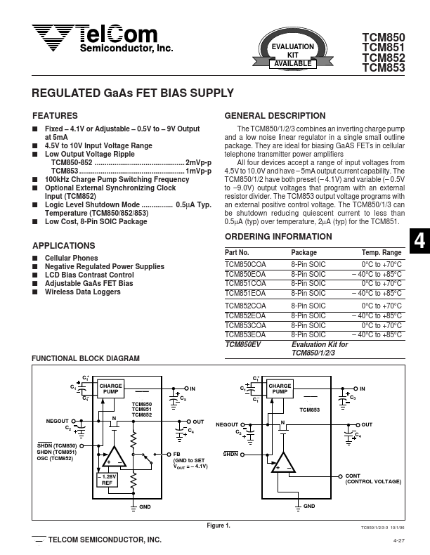
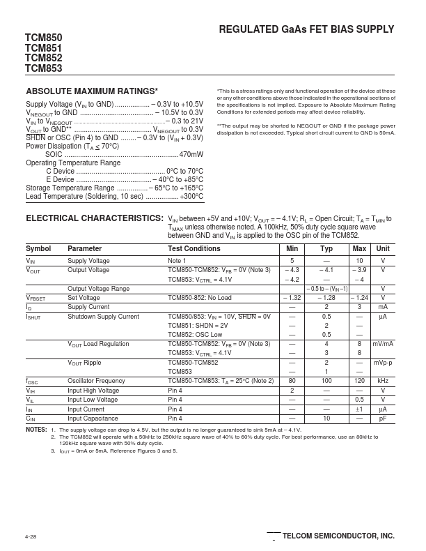
The TCM850/1/2/3 bines an inverting charge pump and a low noise linear regulator in a single small outline package. They are ideal for biasing GaAS FETs in cellular telephone transmitter power amplifiers All four devices accept a range of input voltages from 4.5V to 10.0V and have 5mA output current capability. The TCM850/1/2 have both preset ( 4.1V) and variable ( 0.5V to 9.0V) output voltages that program with an...
TCM851 Key Features
- 4.1V or Adjustable
- 9V Output at 5mA 4.5V to 10V Input Voltage Range Low Output Voltage Ripple TCM850-852
- 2mVp-p TCM853
- 1mVp-p 100kHz Charge Pump Switching Frequency Optional External Synchronizing Clock Input (TCM852) Logic Level Shutdown
- 0.5µA Typ. Temperature (TCM850/852/853) Low Cost, 8-Pin SOIC Package
TCM851 Applications
- 40°C to +85°C 0°C to +70°C