TelCom Semiconductor TCM852
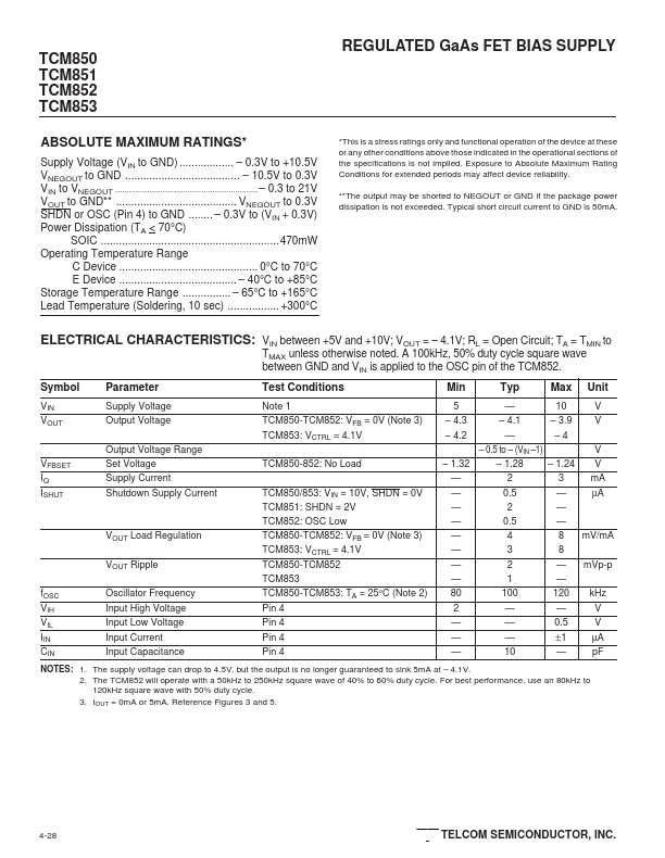
The TCM852 will operate with a 50kHz to 250kHz square wave of 40% to 60% duty cycle. For best performance, use an 80kHz to 120kHz square wave with 50% duty cycle.| Part No. | TCM852 |
|---|---|
| Datasheet | TCM852 Download |
| Manufacturer |  TelCom Semiconductor |
| Description | REGULATED GaAs FET BIAS SUPPLY |
| Buy | Stock & Price |

FEATURES
s s s Fixed – 4.1V or Adjustable – 0.5V to – 9V Output at 5mA 4.5V to 10V Input Voltage Range Low Output Voltage Ripple TCM850-852 .............................................. 2mVp-p TCM853 ...................................................... 1mVp-p 100kHz Charge Pump Switching Frequency Optional External Synchronizing Clock Input (TCM852) Logic Level Shutdown Mode ................ 0.5µA Typ. Temperature (TCM850/852/853) Low Cost, 8-Pin SOIC PackageGENERAL DESCRIPTION
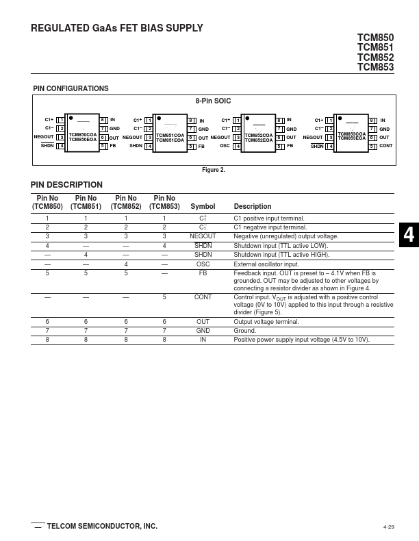
The TCM850/1/2/3 combines an inverting charge pump and a low noise linear regulator in a single small outline package. They are ideal for biasing GaAS FETs in cellular telephone transmitter power amplifiers All four devices accept a range of input voltages from 4.5V to 10.0V and have – 5mA output current capability. The TCM850/1/2 have both preset (– 4.1V) and variable (– 0.5V to –9.0V) output voltages that program with an external resistor divider. The TCM853 output voltage programs with an external positive control voltage.