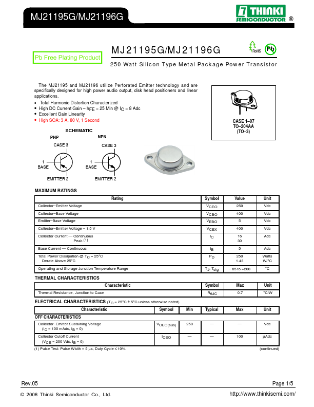
MAXIMUM RATINGS
Rating Collector–Emitter Voltage Collector–Base Voltage Emitter–Base Voltage Collector–Emitter Voltage – 1.5 V Collector Current — Continuous Collector Current — Peak (1) Base Current — Continuous Total Power Dissipation @ TC = 25°C Derate Above 25°C Operating and Storage Junction Temperature Range THERMAL CHARACTERISTICS Characteristic Thermal Resistance, Junction to Case ELECTRICAL CHARACTERISTICS
(TC = 25°C ± 5°C unless otherwise noted) Characteristic Symbol OFF CHARACTERISTICS Collector–Emitter Sustaining Voltage (IC = 100 mAdc, IB = 0) Collector Cutoff Current (VCE = 200 Vdc, IB = 0) (1) Pulse Test: Pulse Width = 5 µs, Duty Cycle ≤ 10%. VCEO(sus) ICEO Min 250 — Symbol VCEO VCBO VEBO VCEX IC IB PD TJ, Tstg Value 250 400 5 400 16 30 5 250 1.43 –āā65 to +200 Unit Vdc Vdc Vdc Vdc Adc Adc Watts W/°C °C Symbol RθJC Max 0.7 Unit °C/W Typical — — Max Unit — Vdc 100 µAdc (continued) Rev.05 © 2006 Thinki Semiconductor Co., Ltd. Page 1/5 MJ21195G/MJ21196G ® ELECTRICAL CHARACT... Thinki Semiconductor