TC59YM916BKG32B Description
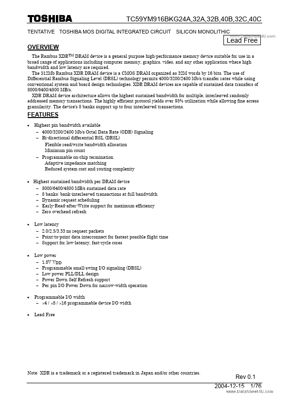
TC59YM916BKG24A,32A,32B,40B,32C,40C TENTATIVE TOSHIBA MOS DIGITAL INTEGRATED CIRCUIT SILICON MONOLITHIC OVERVIEW Lead Free .. The Rambus XDRTM DRAM device is a general purpose high-performance memory device suitable for use in a broad range of applications including puter memory, graphics, video, and any other application where high bandwidth and low latency are required. The 512Mb Rambus XDR DRAM device is a CMOS...
TC59YM916BKG32B Key Features
- Highest pin bandwidth available
- 4000/3200/2400 Mb/s Octal Data Rate (ODR) Signaling
- Bi-directional differential RSL (DRSL) Flexible read/write bandwidth allocation Minimum pin count
- Programmable on-chip termination Adaptive impedance matching Reduced system cost and routing plexity
- Highest sustained bandwidth per DRAM device
- 8000/6400/4800 MB/s sustained data rate 8 banks: bank-interleaved transactions at full bandwidth Dynamic request schedul
- 2.0/2.5/3.33 ns request packets
- Point-to-point data interconnect for fastest possible flight time
- Support for low-latency, fast-cycle cores
- Low power
TC59YM916BKG32B Applications
- Highest pin bandwidth available − 4000/3200/2400 Mb/s Octal Data Rate (ODR) Signaling − Bi-directional differential RSL (DRSL) Flexible read/write bandwidth all
- Highest sustained bandwidth per DRAM device − − − − −
- 8000/6400/4800 MB/s sustained data rate 8 banks: bank-interleaved transactions at full bandwidth Dynamic request scheduling Early-Read-after-Write support for m
- Low power − − − − − 1.8V VDD Programmable small-swing I/O signaling (DRSL) Low power PLL/DLL design Power Down Self Refresh support Per pin I/O Power Down for n


