DF2B6M4SL
Features
(1) Suitable for use with a 5.0 V signal line. (VRWM ≤ 5.5 V) (2) Protects devices with its high ESD performance.
(VESD = ±20 k V (Contact / Air) @IEC61000-4-2) (3) Low dynamic resistance protects semiconductor devices from static electricity and noise.
(RDYN = 0.5 Ω (typ.)) (4) Snapback characteristics realizing low clamping voltage protects semiconductor devices.
(VC = 10 V@IPP = 2 A (typ.)) (5) pact package is suitable for use in high density board layouts such as in mobile devices.
(0.32 × 0.62 mm size (Toshiba package name: SL2))
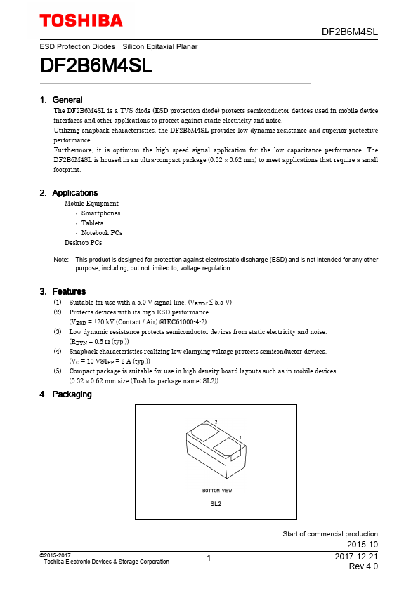
4. Packaging
SL2
©2015-2017 Toshiba Electronic Devices & Storage Corporation
Start of mercial production
2015-10
2017-12-21 Rev.4.0
5. Example of Circuit Diagram
6. Quick Reference Data
Characteristics
Symbol Note
Test Condition
Min Typ. Max Unit
Working peak reverse voltage
Total capacitance
Dynamic resistance
Electrostatic discharge voltage (IEC61000-4-2) (Contact)
VRWM Ct
RDYN VESD
(Note 1)
VR = 0 V, f = 1...