K12A60D Overview
Key Specifications
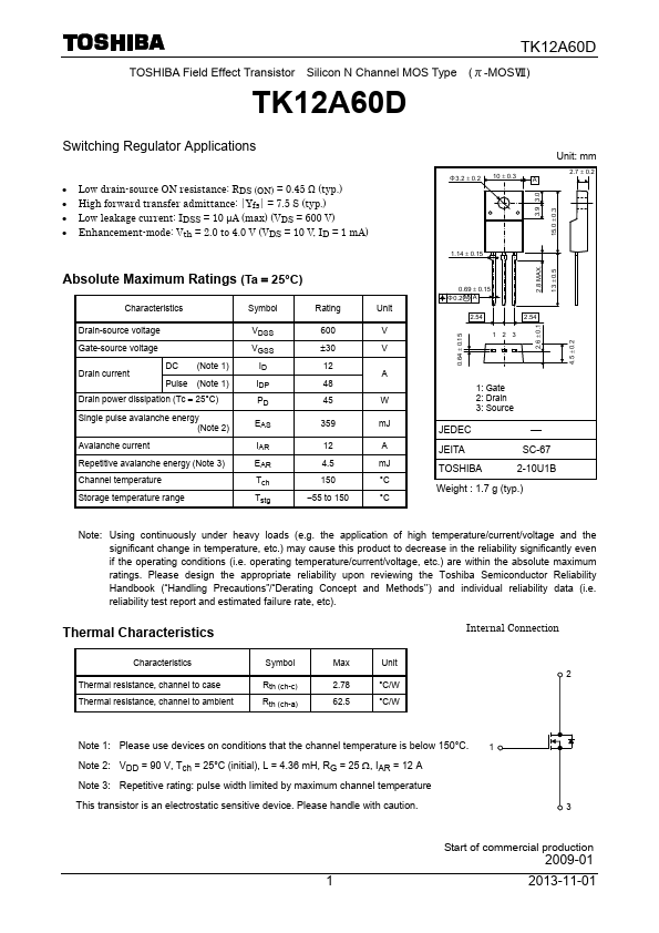
Package: TO-220-3
Mount Type: Through Hole
Pins: 3
Max Operating Temp: 150 °C
Key Features
- Low drain-source ON resistance: RDS (ON) = 0.45 Ω (typ.) High forward transfer admittance: ⎪Yfs⎪ = 7.5 S (typ.) Low leakage current: IDSS = 10 μA (max) (VDS = 600 V) Enhancement-mode: Vth = 2.0 to 4.0 V (VDS = 10 V, ID = 1 mA)