SSM3J56MFV Overview
Key Specifications
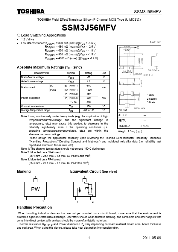
Package: SOT-723
Mount Type: Surface Mount
Max Operating Temp: 150 °C
Key Features
- 1.2 V drive Low ON-resistance:RDS(ON) = 390 mΩ (max) (@VGS = -4.5 V) RDS(ON) = 480 mΩ (max) (@VGS = -2.5 V) RDS(ON) = 660 mΩ (max) (@VGS = -1.8 V) RDS(ON) = 900 mΩ (max) (@VGS = -1.5 V) RDS(ON) = 4000 mΩ (max) (@VGS = -1.2 V) Unit: mm