SSM6N09FU
Description
SSM6N09FU TOSHIBA Field Effect Transistor Silicon N Channel MOS Type SSM6N09FU High Speed Switching Applications Unit: mm • Small package • Low Drain-Source ON resistance. : Ron = 0.7 Ω (max) (@VGS...
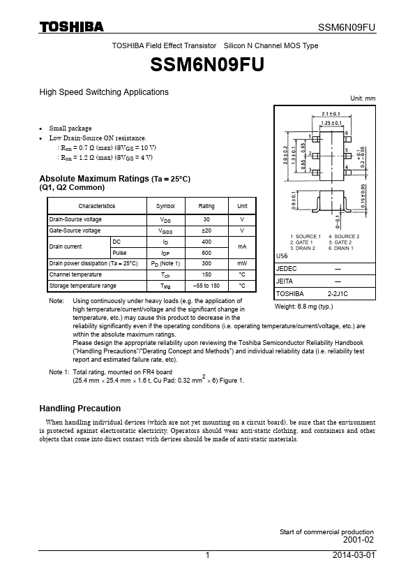
SSM6N09FU TOSHIBA Field Effect Transistor Silicon N Channel MOS Type SSM6N09FU High Speed Switching Applications Unit: mm • Small package • Low Drain-Source ON resistance. : Ron = 0.7 Ω (max) (@VGS...