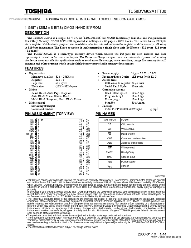
Datasheet4U Logo Datasheet4U.com

TC58DVG02A1FT00 - MOS DIGITAL INTEGRATED CIRCUIT SILICON GATE CMOS

General Description

The TC58DVG02A1 is a single 3.3 V 1-Gbit (1,107,296,256) bit NAND Electrically Erasable and Programmable Read-Only Memory (NAND E2PROM) organized as 528 bytes u 32 pages u 8192 blocks.

Key Features

  • x Organization Memory cell allay 528 u 256K u 8 Register 528 u 8 Page size 528 bytes Block size (16K  512) bytes x Modes Read, Reset, Auto Page Program, Auto Block Erase, Status Read, Multi Block Program, Multi Block Erase x Mode control Serial input/output Command control x Power supply VCC 2.7 V to 3.6 V x Program/Erase Cycles 1E5 cycle (with ECC) x Access time Cell array to register 25 Ps max Serial Read Cycle 50 ns min x Operating current Read (50 ns cycle) 10 mA typ. Program (avg. ).

📥 Download Datasheet

Datasheet Details

Part number TC58DVG02A1FT00
Manufacturer Toshiba
File Size 511.12 KB
Description MOS DIGITAL INTEGRATED CIRCUIT SILICON GATE CMOS
Datasheet download datasheet TC58DVG02A1FT00 Datasheet

Full PDF Text Transcription (Reference)

The following content is an automatically extracted verbatim text from the original manufacturer datasheet and is provided for reference purposes only.

View original datasheet text
TC58DVG02A1FT00 www.DataSheet4U.com TENTATIVE TOSHIBA MOS DIGITAL INTEGRATED CIRCUIT SILICON GATE CMOS 2 1-GBIT (128M u 8 BITS) CMOS NAND E PROM DESCRIPTION The TC58DVG02A1 is a single 3.3 V 1-Gbit (1,107,296,256) bit NAND Electrically Erasable and Programmable Read-Only Memory (NAND E2PROM) organized as 528 bytes u 32 pages u 8192 blocks. The device has a 528-byte static register which allows program and read data to be transferred between the register and the memory cell array in 528-byte increments. The Erase operation is implemented in a single block unit (16 Kbytes  512 bytes: 528 bytes u 32 pages). The TC58DVG02A1 is a serial-type memory device which utilizes the I/O pins for both address and data input/output as well as for command inputs.