TC74AC11FN
TC74AC11FN is Triple 3-Input AND Gate manufactured by Toshiba.
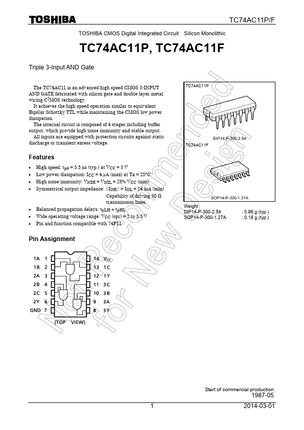
Features
- High speed: tpd = 5.3 ns (typ.) at VCC = 5 V
- Low power dissipation: ICC = 4 μA (max) at Ta = 25°C
- High noise immunity: VNIH = VNIL = 28% VCC (min)
- Symmetrical output impedance: |IOH| = IOL = 24 m A (min)
Capability of driving 50 Ω transmission lines.
- Balanced propagation delays: tp LH ∼- tp HL
- Wide operating voltage range: VCC (opr) = 2 to 5.5 V
- Pin and function patible with 74F11
Pin Assignment
Note: xxx FN (JEDEC SOP) is not available in Japan.
TC74AC11P
TC74AC11F
Weight DIP14-P-300-2.54 SOP14-P-300-1.27A SOL14-P-150-1.27
: 0.96 g (typ.) : 0.18 g (typ.) : 0.12 g (typ.)
1 2007-10-01
IEC Logic Symbol
TC74AC11P/F/FN
Truth Table
LXX XLX XXL HHH
X: Don’t care
Absolute Maximum Ratings (Note 1)
Characteristics
Symbol
Rating
Unit
Supply voltage range DC input voltage DC output voltage Input diode current Output diode current DC output current DC VCC/ground current Power dissipation Storage temperature
VCC VIN VOUT IIK IOK IOUT ICC PD Tstg
- 0.5 to 7.0
- 0.5 to VCC + 0.5
- 0.5 to VCC + 0.5
±20 ±50 ±50 ±100 500 (DIP) (Note 2)/180 (SOP)
- 65 to 150
V V V m A m A m A m A m W °C
Note 1:
Exceeding any of the absolute maximum ratings, even briefly, lead to deterioration in IC performance or even destruction. Using continuously under heavy loads (e.g. the application of high temperature/current/voltage and the significant change in temperature, etc.) may cause this product to decrease in the reliability significantly even if the operating conditions (i.e. operating temperature/current/voltage, etc.) are within the absolute maximum ratings and the operating ranges. Please design the appropriate reliability upon reviewing the Toshiba Semiconductor Reliability Handbook (“Handling Precautions”/Derating Concept and Methods) and individual reliability data (i.e. reliability test report and estimated failure rate, etc).
Note 2: 500 m W in the range of Ta =
- 40 to 65°C. From Ta = 65 to 85°C a derating factor...