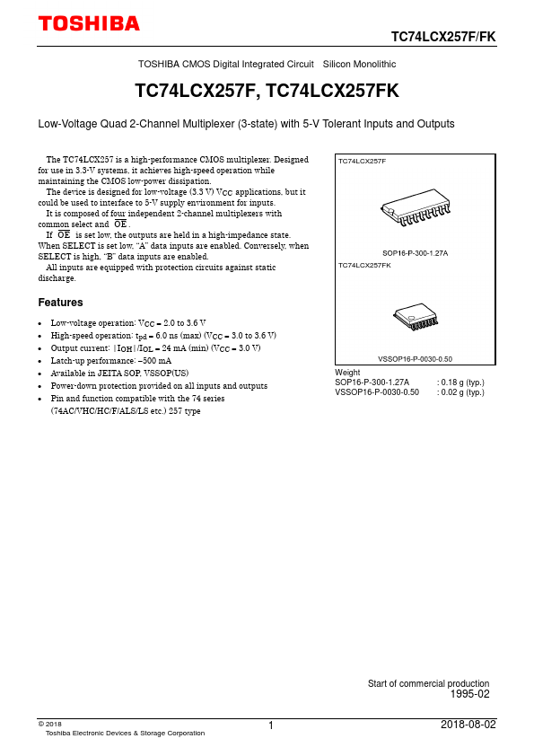
TC74LCX257F
Features
- Low-voltage operation: VCC = 2.0 to 3.6 V
- High-speed operation: tpd = 6.0 ns (max) (VCC = 3.0 to 3.6 V)
- Output current: |IOH|/IOL = 24 m A (min) (VCC = 3.0 V)
- Latch-up performance:
- 500 m A
- Available in JEITA SOP, VSSOP(US)
- Power-down protection provided on all inputs and outputs
- Pin and function patible with the 74 series
(74AC/VHC/HC/F/ALS/LS etc.) 257 type
TC74LCX257F TC74LCX257FK
Weight SOP16-P-300-1.27A VSSOP16-P-0030-0.50
: 0.18 g (typ.) : 0.02 g (typ.)
© 2018
Toshiba Electronic Devices & Storage Corporation
Start of mercial production
1995-02
2018-08-02
Pin Assignment (top view)
SELECT 1 1A 2 1B 3 1Y 4 2A 5 2B 6 2Y 7
GND 8
16 VCC 15 14 4A 13 4B 12 4Y 11 3A 10 3B 9 3Y
Truth Table
Inputs
SELECT...