Datasheet Summary
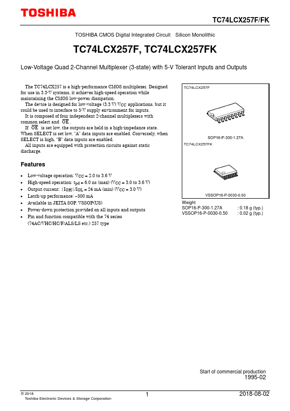
TC74LCX257F/FK
TOSHIBA CMOS Digital Integrated Circuit Silicon Monolithic
TC74LCX257F, TC74LCX257FK
Low-Voltage Quad 2-Channel Multiplexer (3-state) with 5-V Tolerant Inputs and Outputs
The TC74LCX257 is a high-performance CMOS multiplexer. Designed for use in 3.3-V systems, it achieves high-speed operation while maintaining the CMOS low-power dissipation.
The device is designed for low-voltage (3.3 V) VCC applications, but it could be used to interface to 5-V supply environment for inputs.
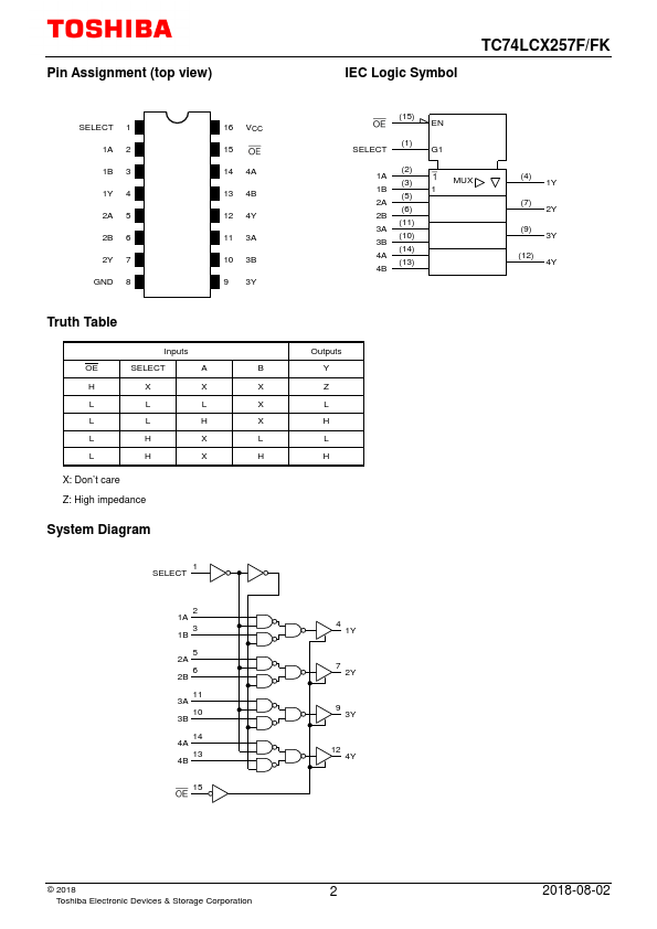
It is posed of four independent 2-channel multiplexers with mon select and OE .
If OE is set low, the outputs are held in a high-impedance state. When SELECT is set low, “A” data inputs are...