TK12J60W
Overview
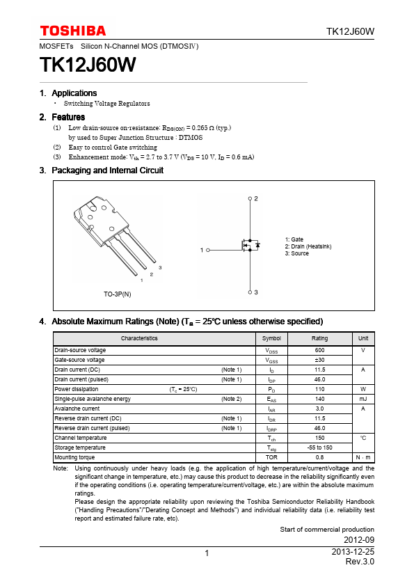
- Packaging and Internal Circuit 1: Gate 2: Drain (Heatsink) 3: Source TO-3P(N)
| Part Number | Manufacturer | Description |
|---|---|---|
| TK12J60W | Inchange Semiconductor | N-Channel MOSFET |
| TK12J60U | Inchange Semiconductor | N-Channel MOSFET |