TK65G10N1
TK65G10N1 is Silicon N-Channel MOSFET manufactured by Toshiba.
Features
(1) (2) (3) Low drain-source on-resistance: RDS(ON) = 3.8 mΩ (typ.) (VGS = 10 V) Low leakage current: IDSS = 10 µA (max) (VDS = 100 V) Enhancement mode: Vth = 2.0 to 4.0 V (VDS = 10 V, ID = 1.0 m A)
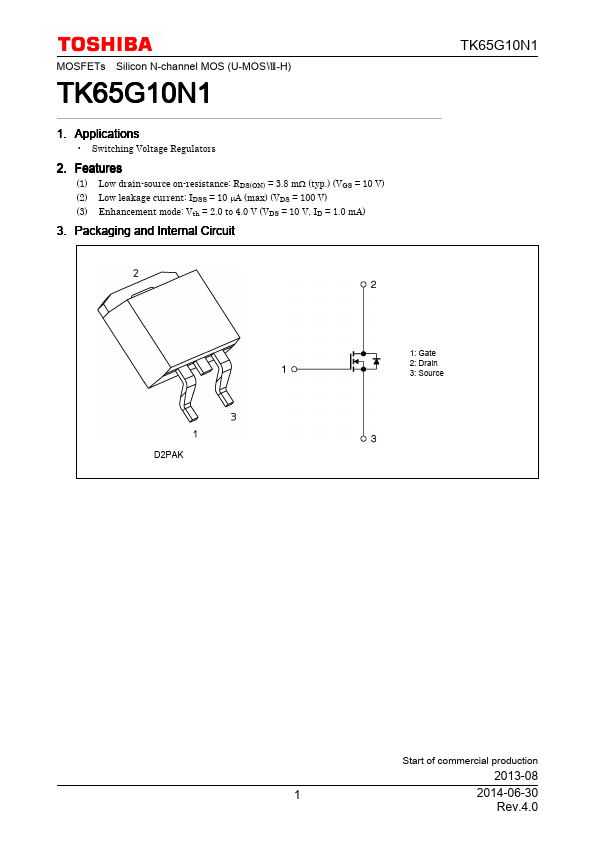
3. Packaging and Internal Circuit
1: Gate 2: Drain 3: Source
D2PAK
Start of mercial production
2013-08 2014-06-30 Rev.4.0
4. Absolute Maximum Ratings (Note) (Ta = 25 unless otherwise specified)
Characteristics Drain-source voltage Gate-source voltage Drain current (DC) Drain current (DC) Drain current (pulsed) Power dissipation Single-pulse avalanche energy Avalanche current Channel temperature Storage temperature (t = 1 ms) (Tc = 25) (Note 4) (Silicon limit) (Note 1, 2) (Note 1, 3) (Note 1) Symbol VDSS VGSS ID ID IDP PD EAS IAR Tch Tstg Rating 100 ±20 136 65 283 156 93 65 150 -55 to 150 W m J A A Unit V
Note:
Using continuously under heavy loads (e.g. the application of high temperature/current/voltage and the significant change in temperature, etc.) may cause this product to decrease in the reliability significantly even if the operating conditions (i.e. operating temperature/current/voltage, etc.) are within the absolute maximum ratings. Please design the appropriate reliability upon reviewing the Toshiba Semiconductor Reliability Handbook ("Handling Precautions"/"Derating Concept and Methods") and individual reliability data (i.e. reliability test report and estimated failure rate, etc).
5. Thermal Characteristics
Characteristics Channel-to-case thermal resistance Symbol Rth(ch-c) Max 0.8 Unit /W
Note 1: Ensure that the channel temperature does not exceed 150. Note 2: Limited by silicon chip capability. Package limit is 100 A. Note 3: Device mounted with heatsink so that Rth(ch-a) bees 2.77/W. Note 4: VDD = 80 V, Tch = 25 (initial), L = 17.1 µH, IAR = 65 A
Note:
This transistor is sensitive to electrostatic discharge and should be handled with care.
2014-06-30 Rev.4.0
6. Electrical Characteristics 6.1. Static...