TB6585AFTG
Description
Motor power supply pin (VM = 4.5 to 42 V) Rotation speed output pin (3 pulses per electrical degree) W-phase Hall-signal input (-) W-phase Hall signal input (+) Signal ground Connection pin for a capacitor to control PWM oscillation Connection pin for a resistor to control PWM oscillation Speed control input Time setting pin for the anti-lock system Rotation direction select input Reset pin for disabling the outputs V-phase Hall-signal input (-) V-phase Hall-signal input (+) U-phase Hall-signal input (-) U-phase Hall-signal input (+) Reference voltage output (Vrefout = 4.4 V (typ.), Irefout =.
Key Features
- Sine-wave PWM drive
- Triangular-wave generator
- Hall amplifier
- Lead angle control
- Current limit control input (VRS = 0.5 V (typ.))
- Rotation pulse output (3 pulse/electrical degree 360°)
- Operating supply voltage range: VM = 4.5 to 42 V
- Reference supply output: Vrefout = 4.4 V (typ.), 20 mA (max)
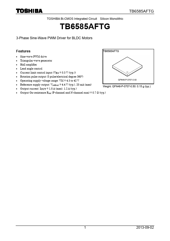
- Output current: IOUT = 1.8 A (max), 1.2 A (typ.) Weight: QFN48-P-0707-0.50: 0.15 g (typ.)
- Output On-resistance Ron (P-channel and N-channel sum) = 0.7 Ω (typ.) 1


