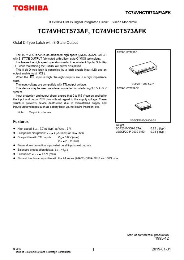
TC74VHCT573AFK Overview
TOSHIBA CMOS Digital Integrated Circuit Silicon Monolithic It achieves the high speed operation similar to equivalent Bipolar Schottky TTL while maintaining the CMOS low power dissipation. This 8-bit D-type latch is controlled by a latch enable input (LE) and an output enable input ( OE ). When the OE input is high, the eight outputs are in a high impedance state. The input voltage are patible with TTL output voltage. This device may be used as a level converter for interfacing 3.3 V to 5 V system. Input protection and output circuit ensure that 0 to 5.5 V can be applied to the input and output (Note) pins without regard to the supply voltage. These structure prevents device destruction due to mismatched supply and input/output voltages such as battery back up, hot board insertion, etc. Note: Output in off-state TC74VHCT573AF TC74VHCT573AFK Features 2019-01-31 Pin Assignment...
TC74VHCT573AFK Key Features
- High speed: tpd 7.7 ns (typ.) at VCC 5 V
- Low power dissipation: ICC 4 A (max) at Ta 25°C
- patible with TTL inputs
- Power down protection is provided on all inputs and outputs
- Balanced propagation delays: tpLH tpHL
- Low noise: VOLP 1.5 V (max)
- Pin and function patible with the 74 series (74AC/HC/F/ALS/LS etc.) 573 type