Datasheet4U Logo Datasheet4U.com

TC9593XBG Datasheet Automotive Peripheral

Manufacturer: Toshiba

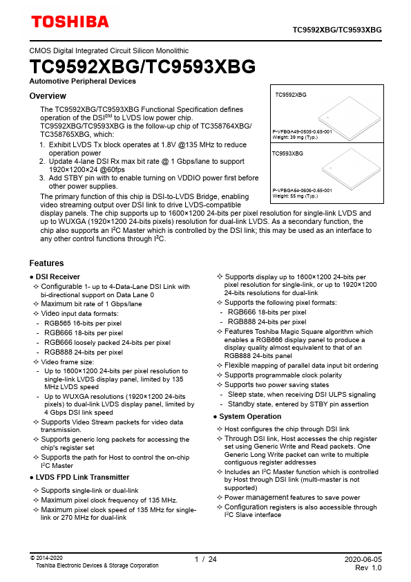
Overview: TC9592XBG/TC9593XBG CMOS Digital Integrated Circuit Silicon Monolithic TC9592XBG/TC9593XBG Automotive Peripheral Devices Overview TC9592XBG The TC9592XBG/TC9593XBG Functional Specification defines operation of the DSISM to LVDS low power chip. TC9592XBG/TC9593XBG is the follow-up chip of TC358764XBG/ TC358765XBG, which: P-VFBGA49-0505-0.65-001 Weight: 39 mg (Typ.) 1. Exhibit LVDS Tx block operates at 1.8V @135 MHz to reduce operation power TC9593XBG 2. Update 4-lane DSI Rx max bit rate @ 1 Gbps/lane to support 1920×1200×24 @60fps 3. Add STBY pin with to enable turning on VDDIO power first before other power supplies. The primary function of this chip is DSI-to-LVDS Bridge, enabling P-VFBGA64-0606-0.65-001 Weight: 55 mg (Typ.) video streaming output over DSI link to drive LVDS-patible display panels. The chip supports up to 1600×1200 24-bits per pixel resolution for single-link LVDS and up to WUXGA (1920×1200 24-bits pixels) resolution for dual-link LVDS. As a secondary function, the chip also supports an I2C Master which is controlled by the DSI link; this may be used as an interface to any other control functions through I2C.

This datasheet includes multiple variants, all published together in a single manufacturer document.

Key Features

  • a Magic Square algorithm which enables a RGB666 display panel to produce a display quality almost equivalent to that of an RGB888 24-bits panel.
  • Flexible mapping of parallel data input bit ordering.
  • Supports programmable clock polarity.
  • Supports two power saving states - Sleep state, when receiving DSI ULPS signaling - Standby state, entered by STBY pin assertion.
  • System Operation.
  • Host configures the chip through DSI link.
  • Through DSI link, Host accesses the chip r.

TC9593XBG Distributor